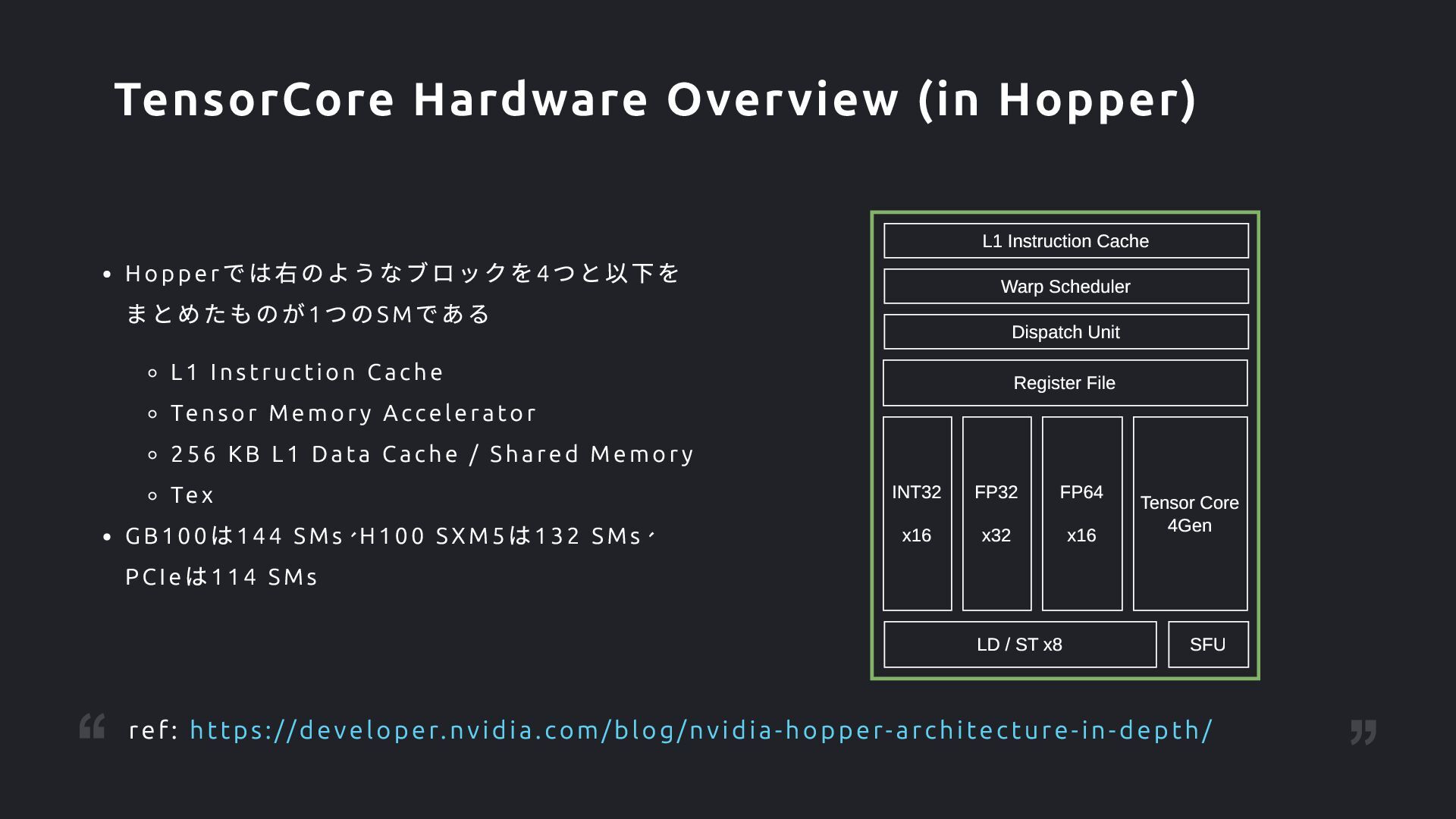
ache Tensor Memor y Accelerato r 256 KB L1 Data C ache / S hare d M emor y Tex GB100 は144 SMs、H100 SX M5 は132 S Ms、 PCIe は114 SMs INT32 x16 FP32 x32 FP64 x16 Tensor Core 4Gen Register File Dispatch Unit Warp Scheduler L1 Instruction Cache SFU LD / ST x8 TensorCore Hardware Overview (in Hopper) ref: https://developer.nvidia.com/blog/nvidia-hopper-architecture-in-depth/
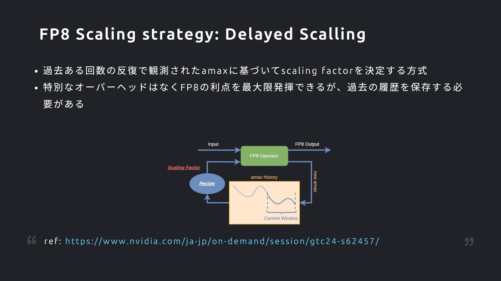
Factor Current Window Recipe amax history new amax Input FP8 Output FP8 Scaling strategy: Delayed Scalling ref: https://w w w.nvidia.com/ja-jp/on-demand/session/gtc24-s62457/
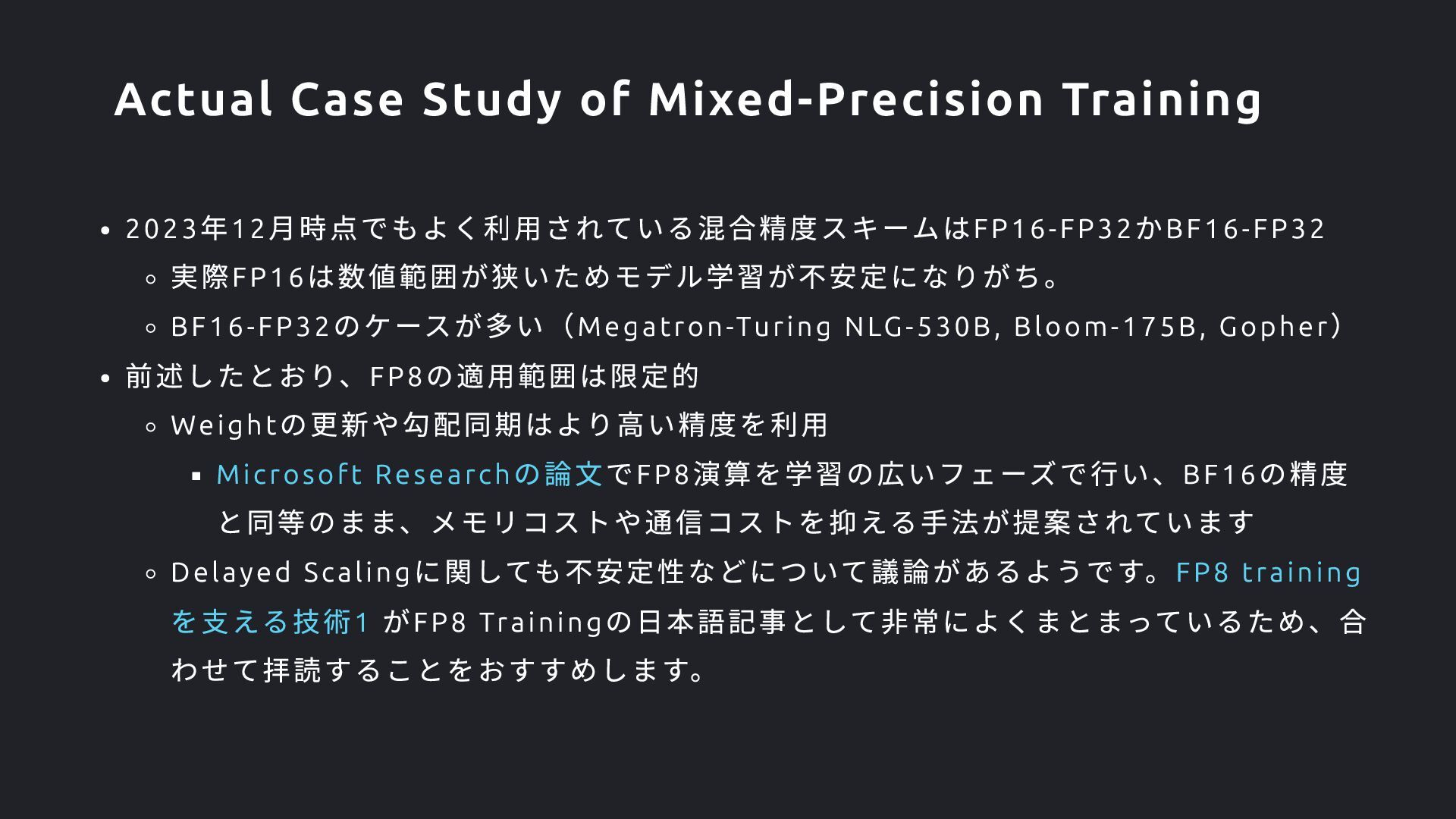
Gopher ) 前述したとおり、FP8 の適用範囲は限定的 Weight の更新や勾配同期はより高い精度を利用 Microsoft Research の論文でFP8 演算を学習の広いフェーズで行い、BF16 の精度 と同等のまま、メモリコストや通信コストを抑える手法が提案されています Delayed Scaling に関しても不安定性などについて議論があるようです。FP8 training を支える技術1 がFP8 Training の日本語記事として非常によくまとまっているため、合 わせて拝読することをおすすめします。 Actual Case Study of Mixed-Precision Training
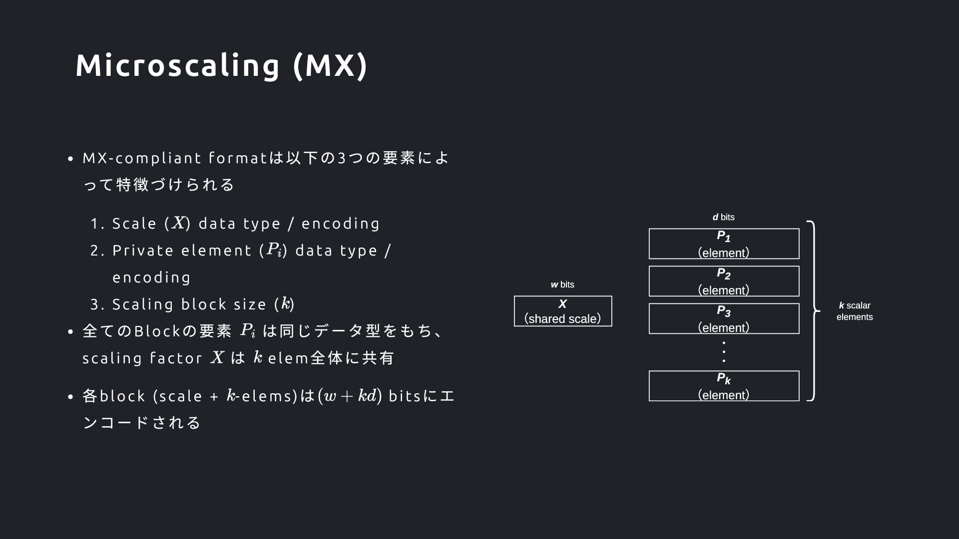
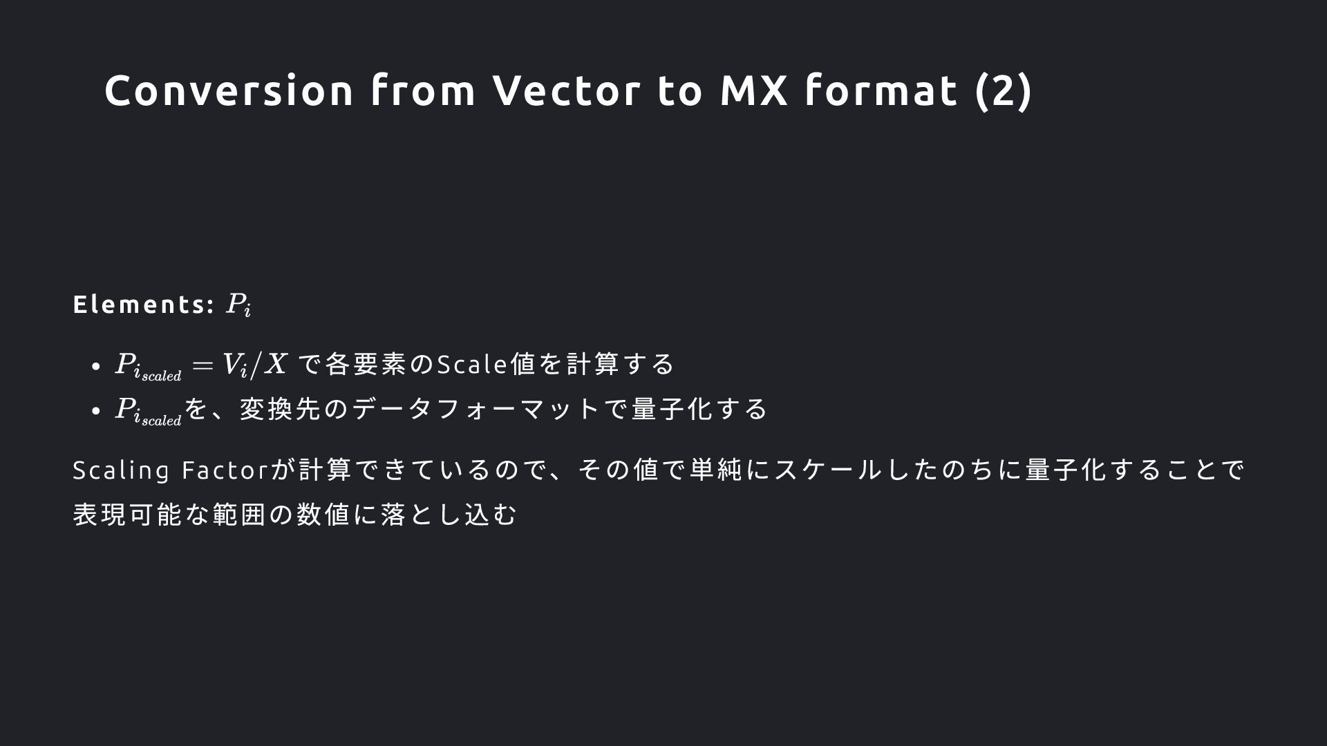
) data t ype / encodi ng 2. Private element ( ) data t ype / encodi ng 3. Scali ng block si ze ( ) 全てのBlock の要素 は同じデータ型をもち、 scali ng factor は elem 全体に共有 各block (scale + - elems) は bi ts にエ ンコードされる X (shared scale) P1 (element) P2 (element) P3 (element) Pk (element) ・・・ w bits d bits k scalar elements Microscaling (MX)
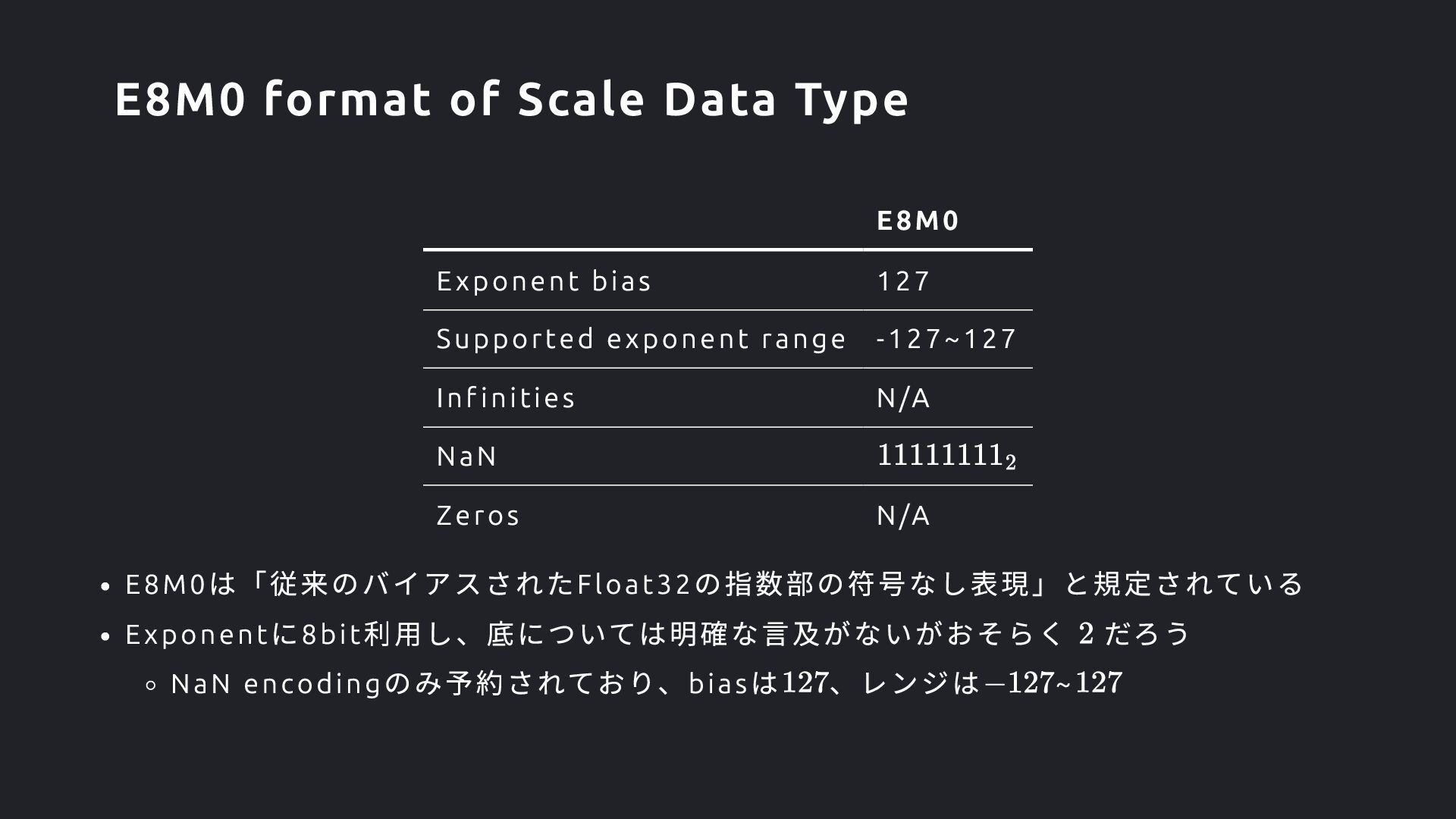
N/A NaN Zeros N/A E8M0 は「従来のバイアスされたFloat32 の指数部の符号なし表現」と規定されている Exponent に8bit 利用し、底については明確な言及がないがおそらく だろう NaN encoding のみ予約されており、bias は 、レンジは ~ E8M0 format of Scale Data Type
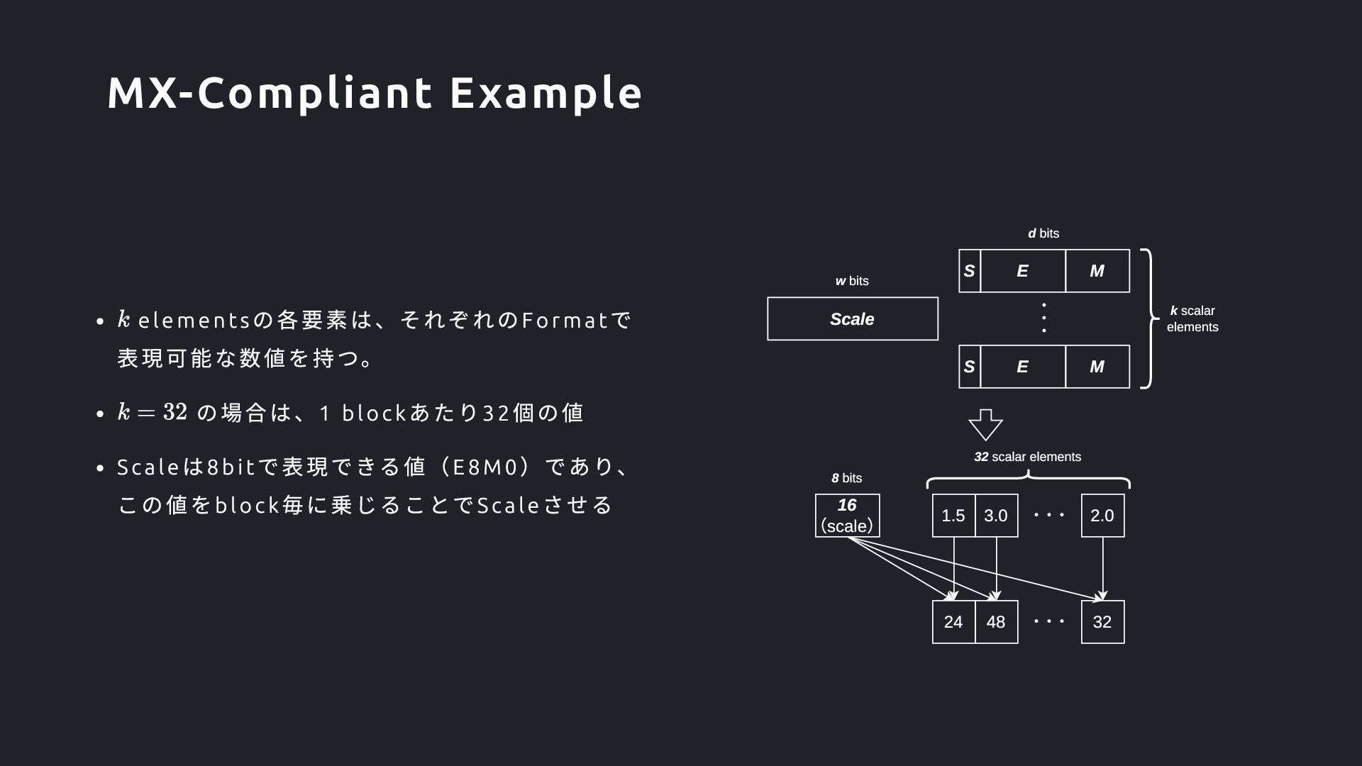
は8bi t で表現できる値(E8M0 )であり、 この値をblock 毎に乗じることでScale させる Scale S ・・・ w bits d bits 32 scalar elements E M S E M 1.5 3.0 2.0 ・・・ 16 (scale) 8 bits 24 48 32 ・・・ k scalar elements MX-Compliant Example
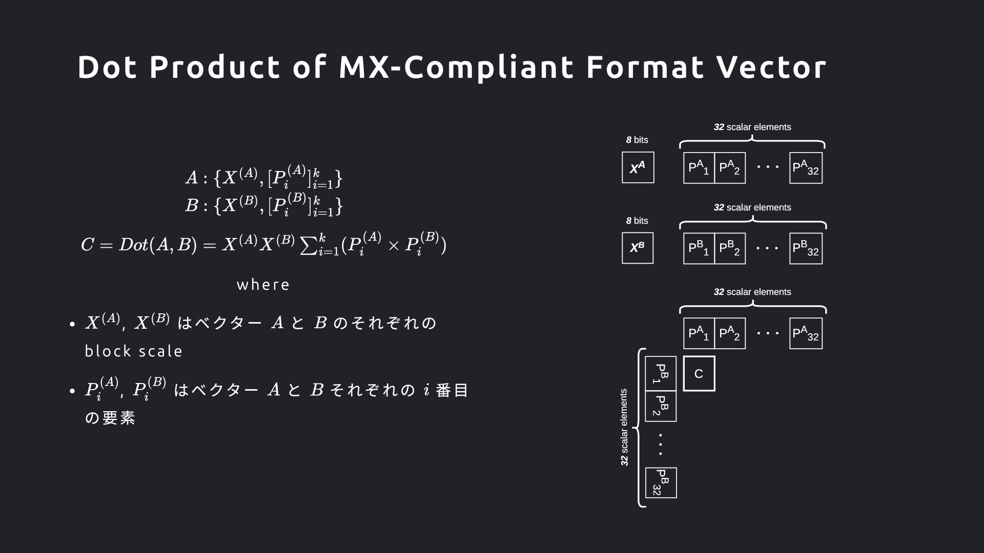
それぞれの 番目 の要素 32 scalar elements PA 1 PA 32 ・・・ XA 8 bits PA 2 32 scalar elements PB 1 PB 32 ・・・ XB 8 bits PB 2 PA 1 PA 32 ・・・ PA 2 PB 1 PB 32 ・・・ PB 2 C 32 scalar elements 32 scalar elements Dot Product of MX-Compliant Format Vector
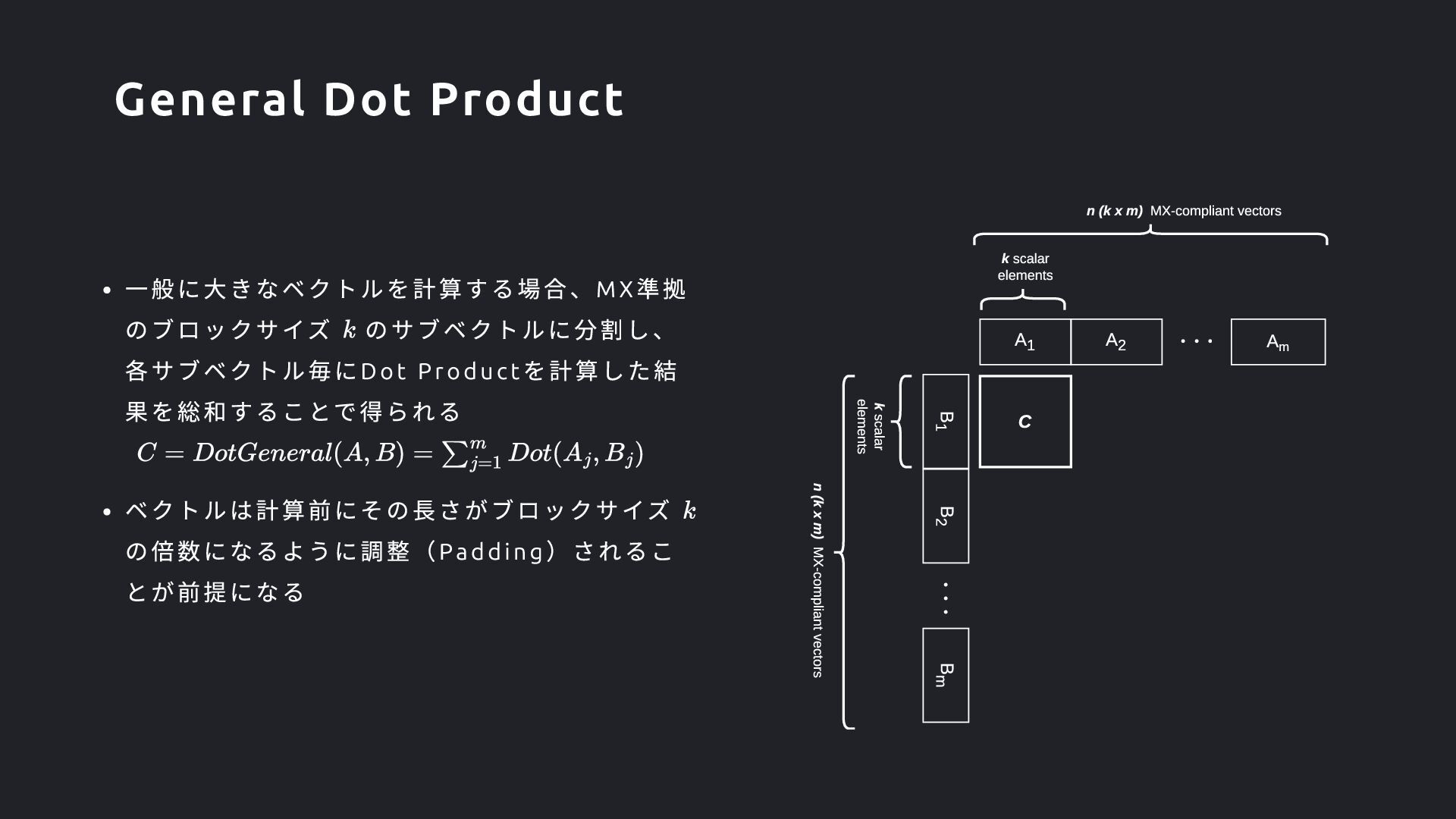
の倍数になるように調整(Padd ing )されるこ とが前提になる B1 C k scalar elements B2 k scalar elements ・・・ Bm A1 A2 ・・・ Am n (k x m) MX-compliant vectors n (k x m) MX-compliant vectors General Dot Product
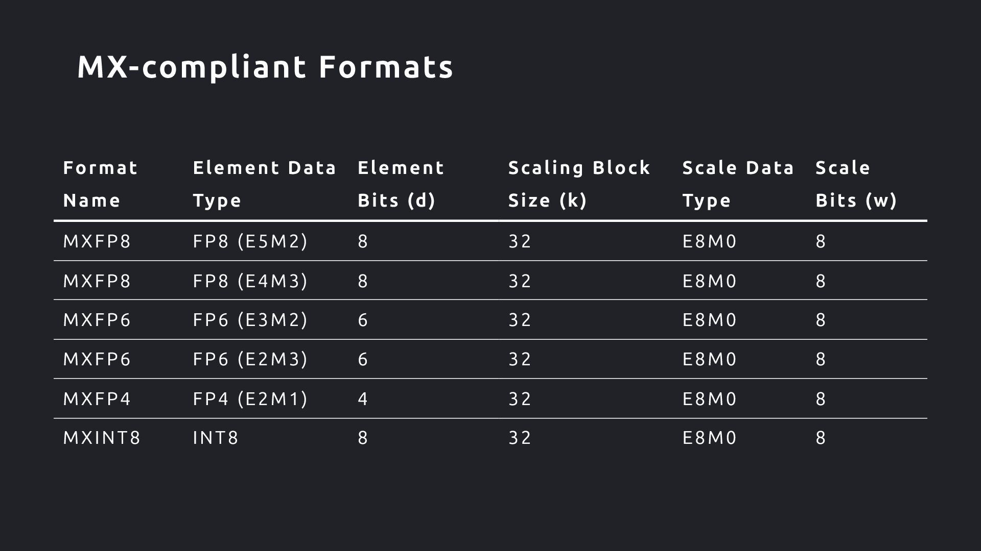
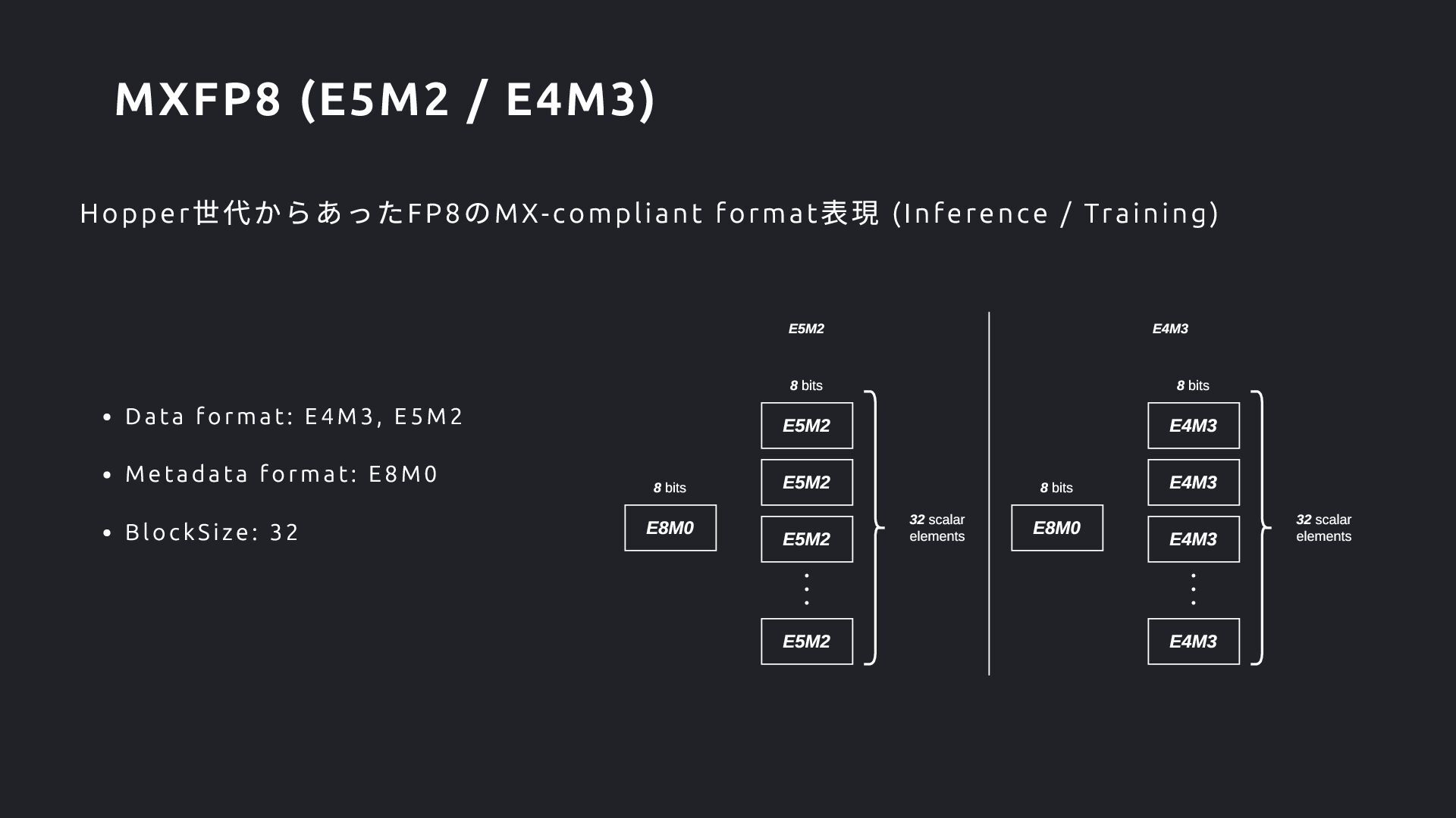
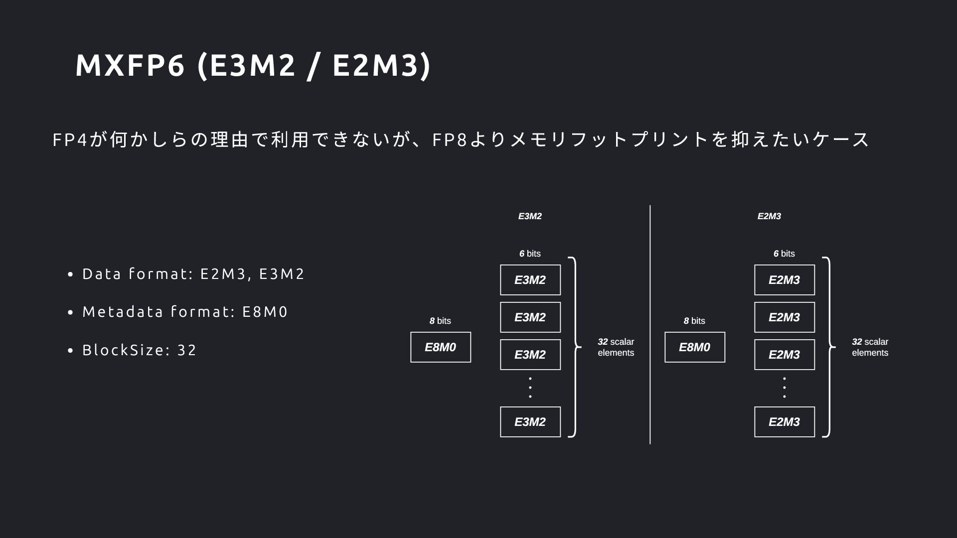
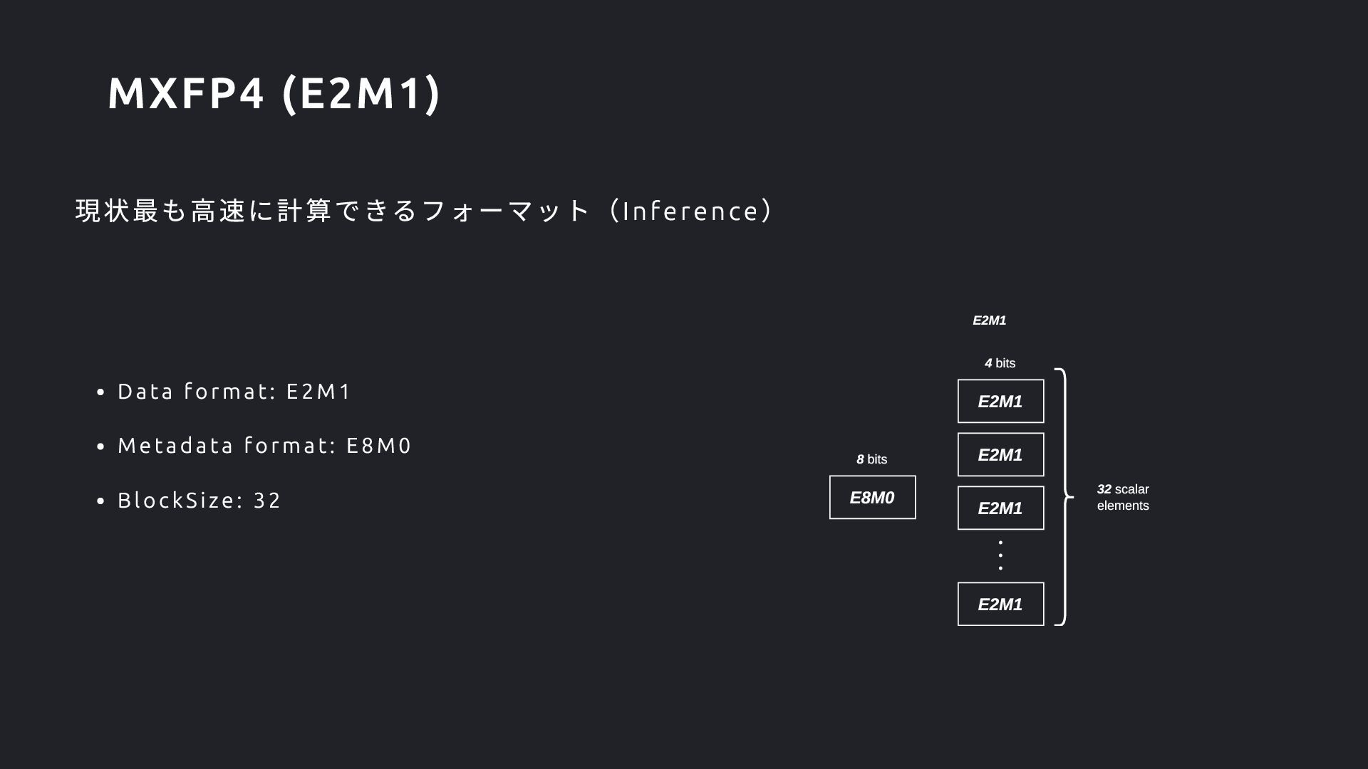
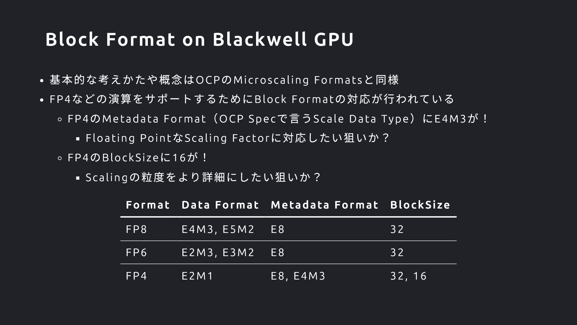
Format (OCP Spec で言うScale Data Type )にE4M3 が! Floating Point なScaling Factor に対応したい狙いか? FP4 のBlockSize に16 が! Scaling の粒度をより詳細にしたい狙いか? Format Data Format Metadata Format BlockSize FP8 E4M3, E5M2 E8 32 FP6 E2M3, E3M2 E8 32 FP4 E2M1 E8, E4M3 32, 16 Block Format on Blackwell GPU
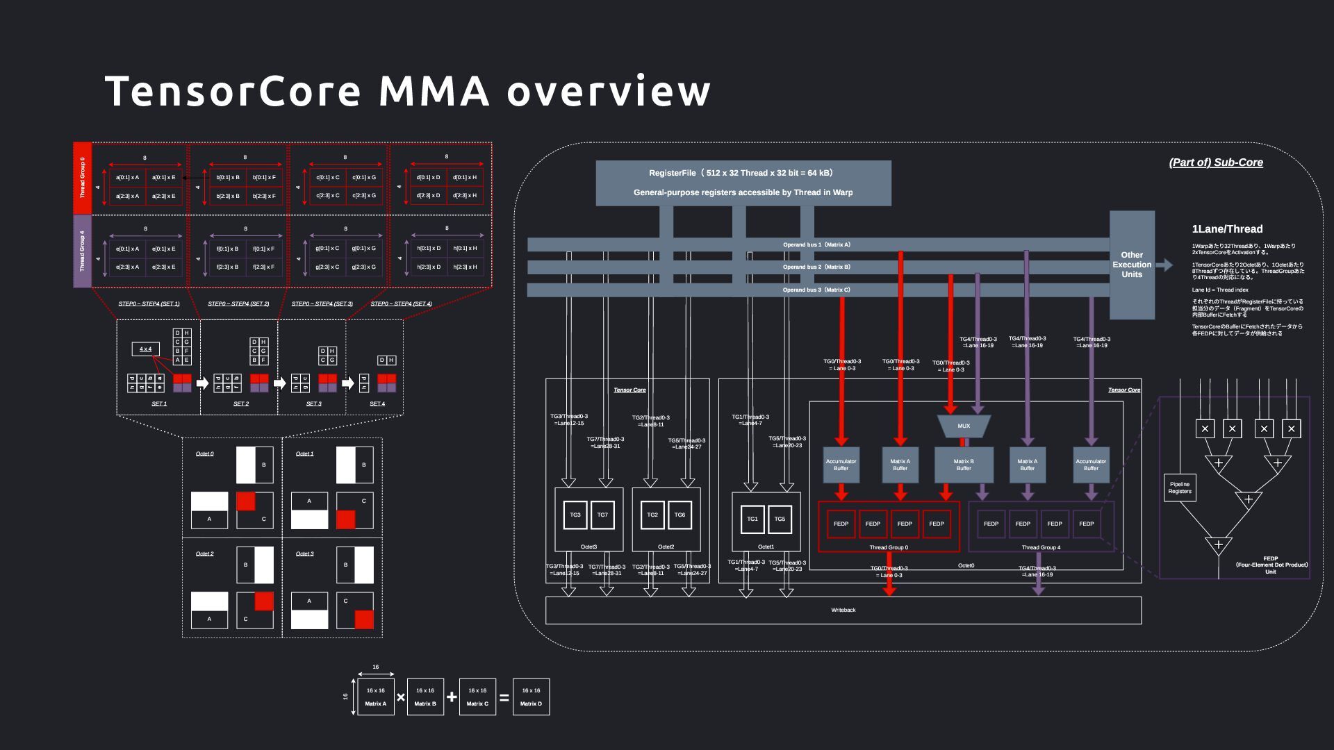
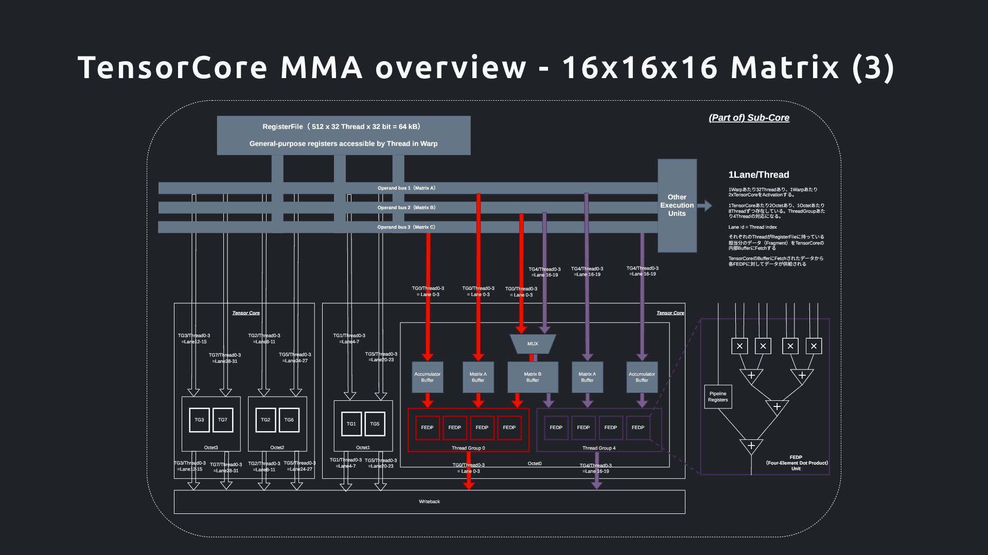
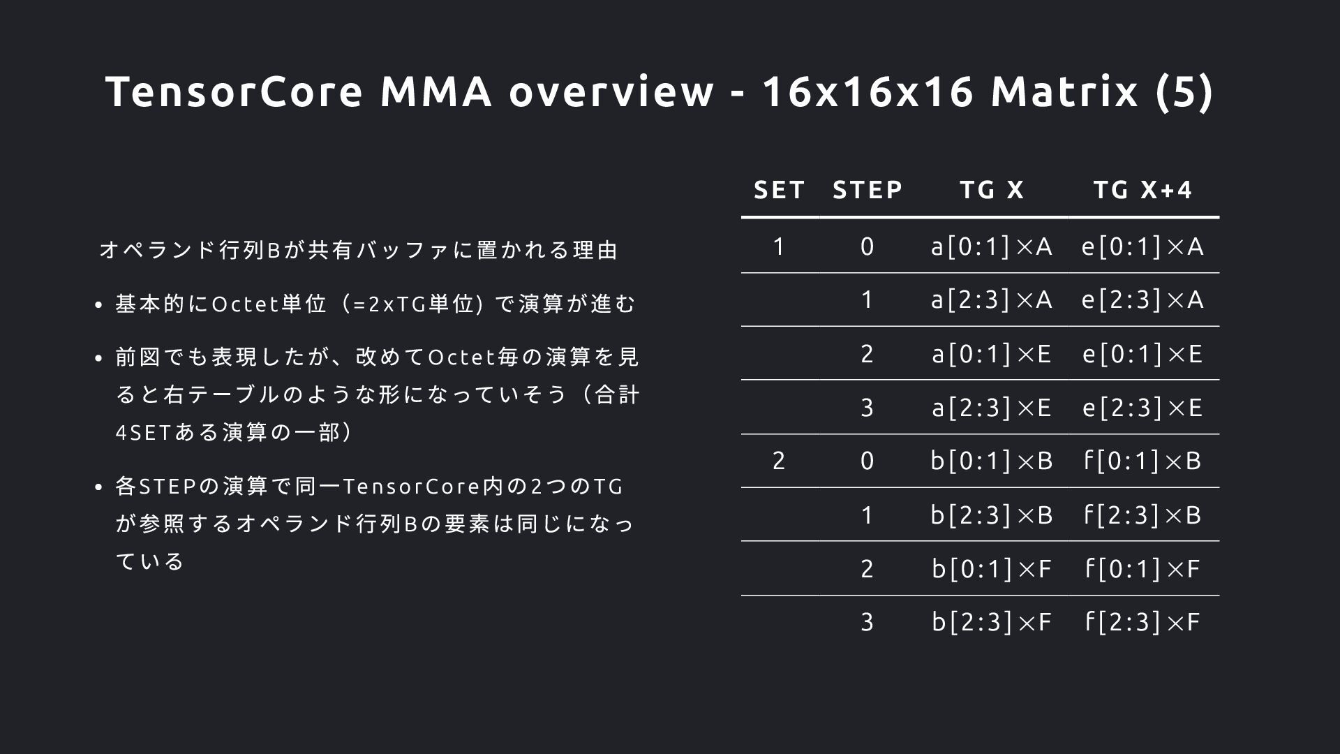
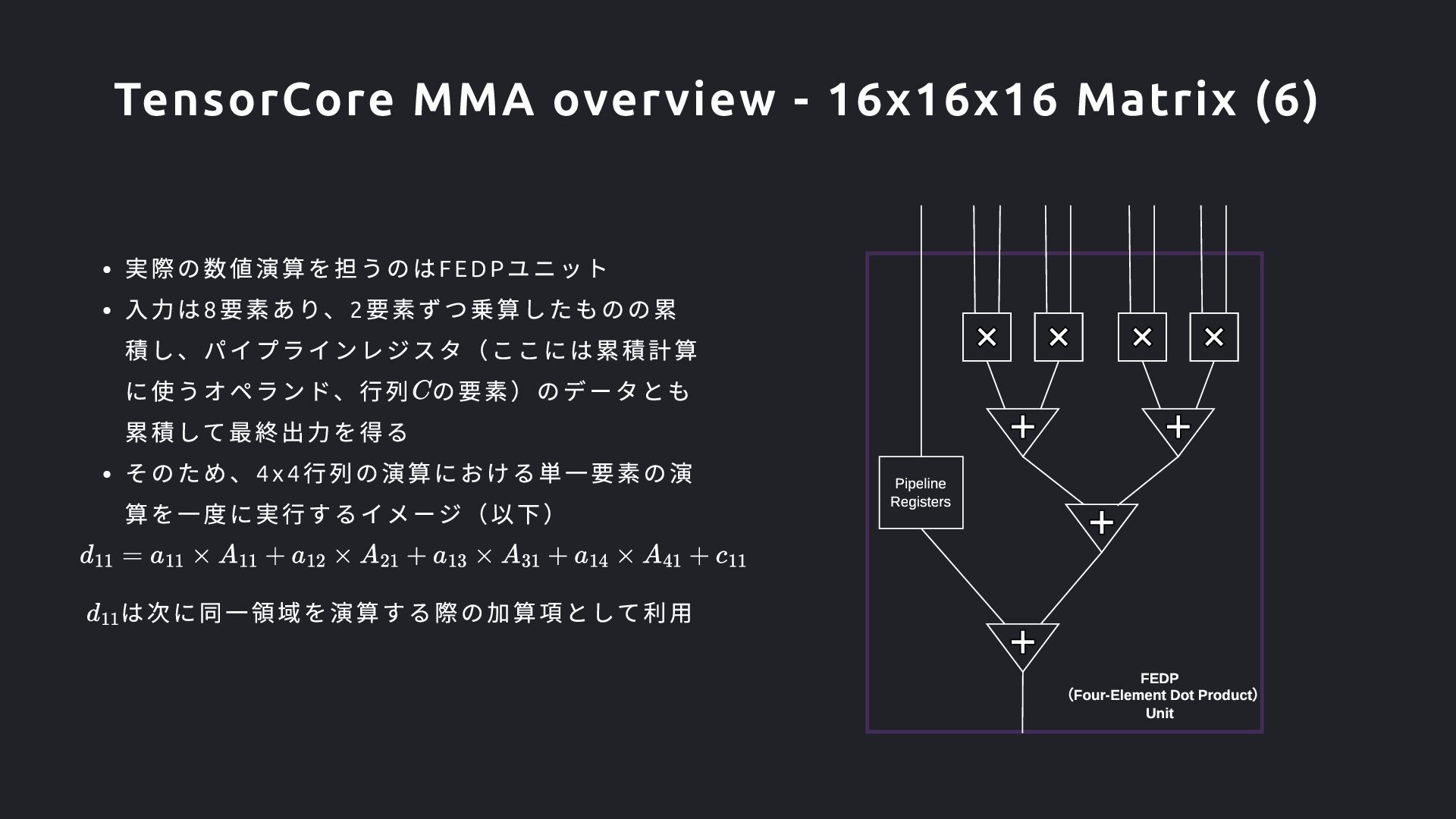
8 4 8 4 8 8 16 16 16 x 16 Matrix A A B C A B C A B C A B C Octet 0 Octet 1 Octet 2 Octet 3 h g f e d c b E B F C G D H h g f d c b B F C G D H h g d c C G D H h d D H SET 1 SET 2 SET 3 SET 4 Thread Group 0 Thread Group 4 e[2:3] x A e[2:3] x E e[0:1] x E e[0:1] x A a[2:3] x A a[2:3] x E a[0:1] x E a[0:1] x A f[2:3] x B f[2:3] x F f[0:1] x F f[0:1] x B b[2:3] x B b[2:3] x F b[0:1] x F b[0:1] x B g[2:3] x C g[2:3] x G g[0:1] x G g[0:1] x C c[2:3] x C c[2:3] x G c[0:1] x G c[0:1] x C h[2:3] x D h[2:3] x H h[0:1] x H h[0:1] x D d[2:3] x D d[2:3] x H d[0:1] x H d[0:1] x D STEP0 ~ STEP4 (SET 1) STEP0 ~ STEP4 (SET 2) STEP0 ~ STEP4 (SET 3) 4 x 4 A a Tensor Core Octet0 Thread Group 0 Thread Group 4 FEDP FEDP FEDP FEDP FEDP FEDP FEDP FEDP Accumulator Buffer Accumulator Buffer Matrix A Buffer Matrix A Buffer MUX Tensor Core Octet3 Octet2 Octet1 TG0/Thread0-3 = Lane 0-3 TG1 TG5 TG2 TG6 TG3 TG7 TG1/Thread0-3 =Lane4-7 TG5/Thread0-3 =Lane20-23 TG2/Thread0-3 =Lane8-11 TG5/Thread0-3 =Lane24-27 TG3/Thread0-3 =Lane12-15 TG7/Thread0-3 =Lane28-31 TG4/Thread0-3 =Lane 16-19 (Part of) Sub-Core Matrix B Buffer 1Lane/Thread 1Warpあたり32Threadあり、1Warpあたり 2xTensorCoreをActivationする。 1TensorCoreあたり2Octetあり、1Octetあたり 8Threadずつ存在している。ThreadGroupあた り4Threadの対応になる。 Lane Id = Thread index それぞれのThreadがRegisterFileに持っている 担当分のデータ(Fragment)をTensorCoreの 内部BufferにFetchする TensorCoreのBufferにFetchされたデータから 各FEDPに対してデータが供給される Other Execution Units Operand bus 3(Matrix C) Operand bus 2(Matrix B) Operand bus 1(Matrix A) TG0/Thread0-3 = Lane 0-3 TG0/Thread0-3 = Lane 0-3 TG4/Thread0-3 =Lane 16-19 TG4/Thread0-3 =Lane 16-19 FEDP (Four-Element Dot Product) Unit Pipeline Registers 16 x 16 Matrix B 16 x 16 Matrix C 16 x 16 Matrix D TG0/Thread0-3 = Lane 0-3 Writeback TG4/Thread0-3 =Lane 16-19 TG1/Thread0-3 =Lane4-7 TG5/Thread0-3 =Lane20-23 TG5/Thread0-3 =Lane24-27 TG2/Thread0-3 =Lane8-11 TG7/Thread0-3 =Lane28-31 TG3/Thread0-3 =Lane12-15 STEP0 ~ STEP4 (SET 4) RegisterFile( 512 x 32 Thread x 32 bit = 64 kB) General-purpose registers accessible by Thread in Warp TensorCore MMA overview
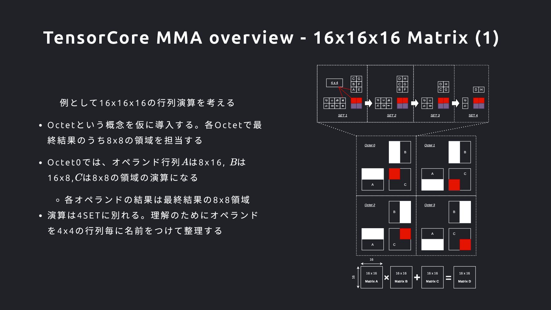
は8x16, は 16x8, は8x8 の領域の演算になる 各オペランドの結果は最終結果の8x8 領域 演算は4SET に別れる。理解のためにオペランド を4x4 の行列毎に名前をつけて整理する 16 16 16 x 16 Matrix A A B C A B C A B C A B C Octet 0 Octet 1 Octet 2 Octet 3 h g f e d c b E B F C G h g f d c b B F C G D H h g d c C G D H h d D H SET 1 SET 2 SET 3 SET 4 4 x 4 A a 16 x 16 Matrix B 16 x 16 Matrix C 16 x 16 Matrix D TensorCore MMA overview - 16x16x16 Matrix (1)
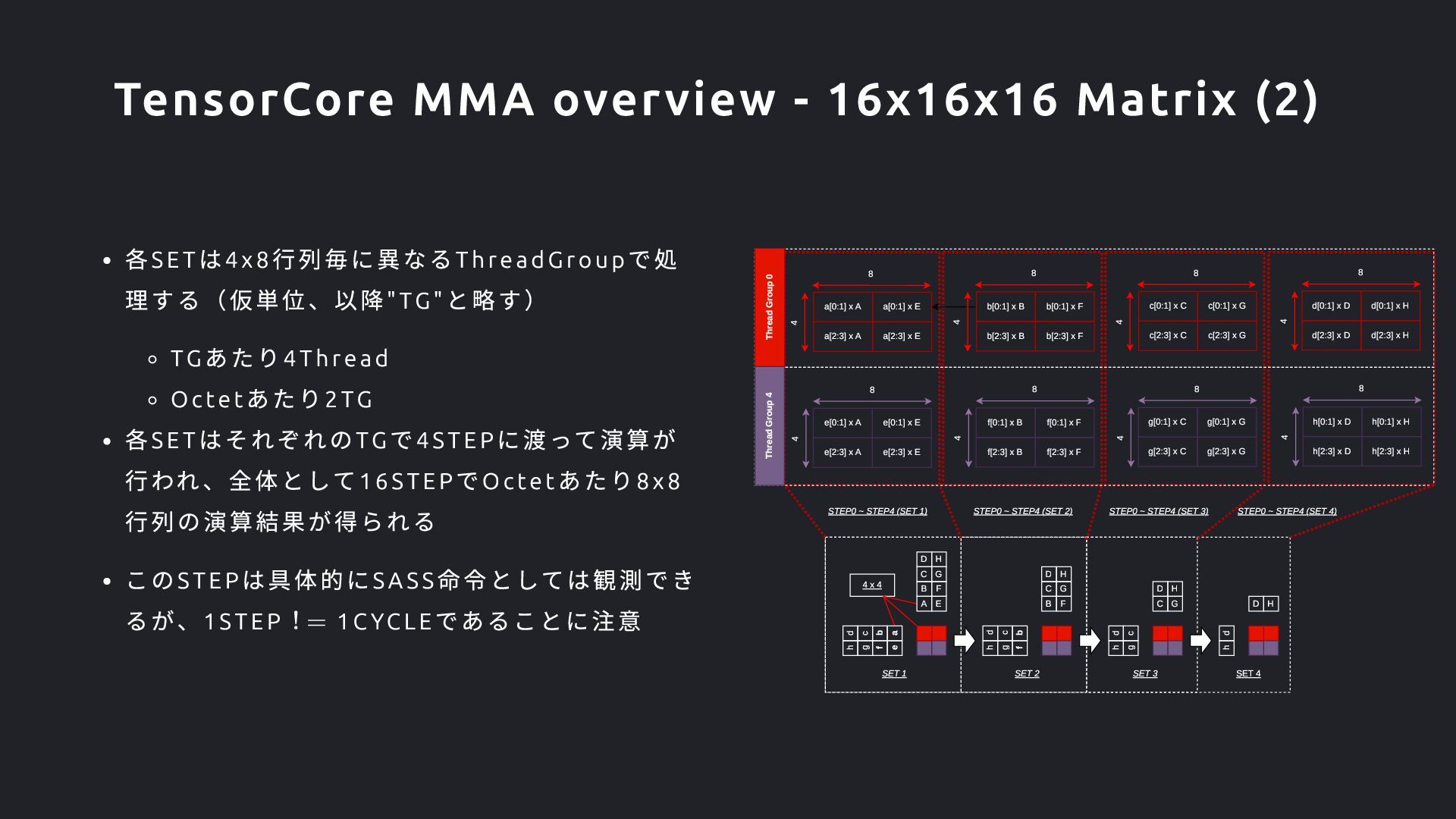
あたり4Thread Octet あたり2TG 各SET はそれぞれのTG で4STEP に渡って演算が 行われ、全体として16STE P でOcte t あたり8x8 行列の演算結果が得られる このSTEP は具体的にSA SS 命令としては観測でき るが、1STEP 1C YCLE であることに注意 4 8 4 8 4 4 8 4 8 4 8 4 8 4 8 8 h g f e d c b E B F C G D H h g f d c b B F C G D H h g d c C G D H h d D H SET 1 SET 2 SET 3 SET 4 Thread Group 0 Thread Group 4 e[2:3] x A e[2:3] x E e[0:1] x E e[0:1] x A a[2:3] x A a[2:3] x E a[0:1] x E a[0:1] x A f[2:3] x B f[2:3] x F f[0:1] x F f[0:1] x B b[2:3] x B b[2:3] x F b[0:1] x F b[0:1] x B g[2:3] x C g[2:3] x G g[0:1] x G g[0:1] x C c[2:3] x C c[2:3] x G c[0:1] x G c[0:1] x C h[2:3] x D h[2:3] x H h[0:1] x H h[0:1] x D d[2:3] x D d[2:3] x H d[0:1] x H d[0:1] x D STEP0 ~ STEP4 (SET 1) STEP0 ~ STEP4 (SET 2) STEP0 ~ STEP4 (SET 3) 4 x 4 A a STEP0 ~ STEP4 (SET 4) TensorCore MMA overview - 16x16x16 Matrix (2)
4SET ある演算の一部) 各STEP の演算で同一TensorCore 内の2 つのTG が参照するオペランド行列B の要素は同じになっ ている SET STEP TG X TG X+4 1 0 a[0:1] A e[0:1] A 1 a[2:3] A e[2:3] A 2 a[0:1] E e[0:1] E 3 a[2:3] E e[2:3] E 2 0 b[0:1] B f[0:1] B 1 b[2:3] B f[2:3] B 2 b[0:1] F f[0:1] F 3 b[2:3] F f[2:3] F TensorCore MMA overview - 16x16x16 Matrix (5)
FP8 training を支える技術 1 Using FP8 with Transformer Engine What's New in Transformer Engine and FP8 Training OCP Microscaling Formats (MX) Specif ication Version 1.0 NVIDIA Blackwell Architecture Technical Brief Blackwell Numerics for AI FP8-LM: Training FP8 Large Language Model References