Upgrade to Pro
— share decks privately, control downloads, hide ads and more …
Speaker Deck
Features
Speaker Deck
PRO
Sign in
Sign up for free
Search
Search
J601_lec03
Search
Ahmad El-Banna
November 02, 2014
Education
990
1
Share
Embed
Copy iframe code
Copy JS code
Copy link
Start on current slide
J601_lec03
5th Year, Integrated Technical Education Cluster AlAmeeria
lec#3, Electronic Principals
Ahmad El-Banna
November 02, 2014
More Decks by Ahmad El-Banna
See All by Ahmad El-Banna
E716_lec12
ahmad_elbanna
0
1.7k
J601_lec12
ahmad_elbanna
1
1k
E716_lec11
ahmad_elbanna
1
650
E716_lec10
ahmad_elbanna
0
600
J601_lec11
ahmad_elbanna
1
1k
J601_lec10
ahmad_elbanna
1
1k
E716_lec09
ahmad_elbanna
0
740
J601_lec09
ahmad_elbanna
0
600
J601_lec08.pdf
ahmad_elbanna
1
1.3k
Other Decks in Education
See All in Education
JAWS-UG初心者支部#81 GWにEduJAWSと何か作ろうもくもく会!
otsuki
0
150
Modern Data Fetching Techniques in Angular
debug_mode
0
230
生成AI時代のエンジニア育成について考えてみた
akasan
0
170
✅ レポート採点基準 / How Your Reports Are Assessed
yasslab
PRO
0
390
Dashboards - Lecture 11 - Information Visualisation (4019538FNR)
signer
PRO
1
2.8k
Visionary Initiative: Future Intelligence 「未来の知性と社会の礎を築く」|Science Tokyo(東京科学大学)
sciencetokyo
PRO
0
810
教育現場から見た Ruby on Rails
yasslab
PRO
0
200
Portable & Reproducible Research Environments in the Age of AI Agents
denkiwakame
0
490
[2026前期火5] 論理学(京都大学文学部 前期 第5回)「 ならばの問題演習・proof net・かつの規則」
yatabe
0
360
アラムコSTEAMチャレンジ 実践報告書
codeforeveryone
0
170
「機械学習と因果推論」入門 ⑤ 因果効果推定の一般化
masakat0
0
150
Stardy 会社紹介資料
stardy
0
2.7k
Featured
See All Featured
The Organizational Zoo: Understanding Human Behavior Agility Through Metaphoric Constructive Conversations (based on the works of Arthur Shelley, Ph.D)
kimpetersen
PRO
0
380
The Director’s Chair: Orchestrating AI for Truly Effective Learning
tmiket
1
210
Understanding Cognitive Biases in Performance Measurement
bluesmoon
32
3k
How to Get Subject Matter Experts Bought In and Actively Contributing to SEO & PR Initiatives.
livdayseo
0
150
Fantastic passwords and where to find them - at NoRuKo
philnash
52
3.8k
Public Speaking Without Barfing On Your Shoes - THAT 2023
reverentgeek
1
460
Scaling GitHub
holman
464
140k
Game over? The fight for quality and originality in the time of robots
wayneb77
1
220
Deep Space Network (abreviated)
tonyrice
0
220
State of Search Keynote: SEO is Dead Long Live SEO
ryanjones
0
220
Writing Fast Ruby
sferik
630
63k
Reality Check: Gamification 10 Years Later
codingconduct
0
2.2k
Transcript
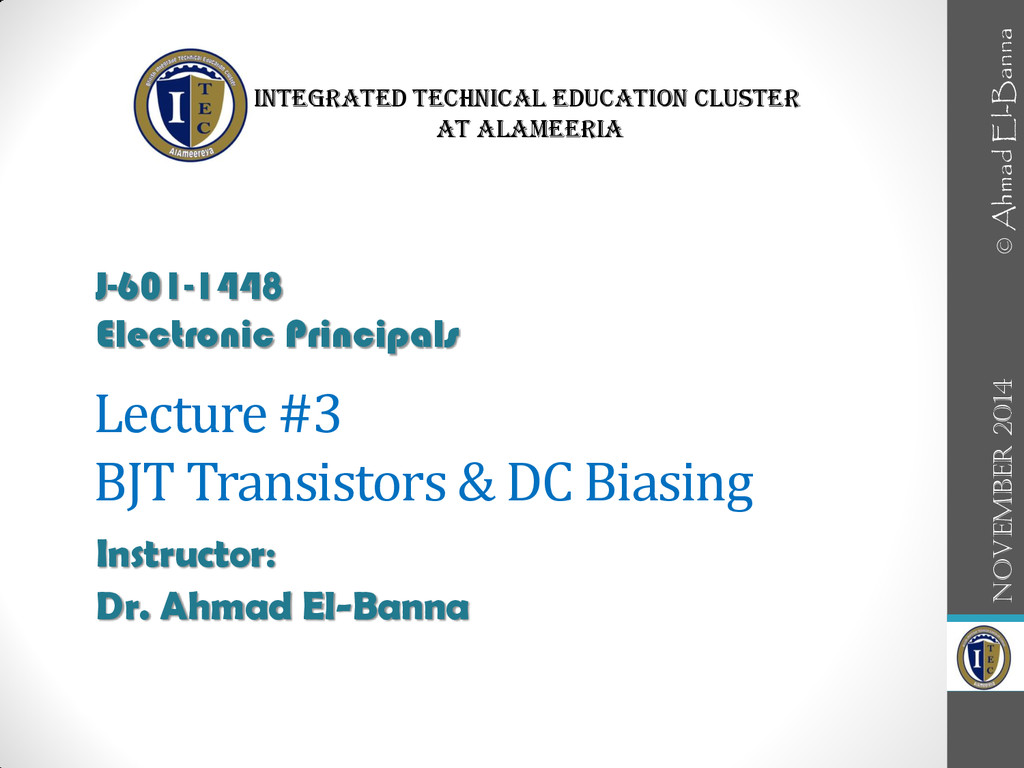
Lecture #3 BJT Transistors & DC Biasing Instructor: Dr. Ahmad
El-Banna November 2014 J-601-1448 Electronic Principals Integrated Technical Education Cluster At AlAmeeria © Ahmad El-Banna
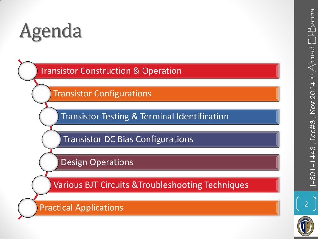
Agenda 2 J-601-1448 , Lec#3 , Nov 2014 © Ahmad
El-Banna Transistor Construction & Operation Transistor Configurations Transistor Testing & Terminal Identification Transistor DC Bias Configurations Design Operations Various BJT Circuits &Troubleshooting Techniques Practical Applications
Transistor Construction • Basic BJT Constructions 3 • Basic BJT
symbols and Currents J-601-1448 , Lec#3 , Nov 2014 © Ahmad El-Banna
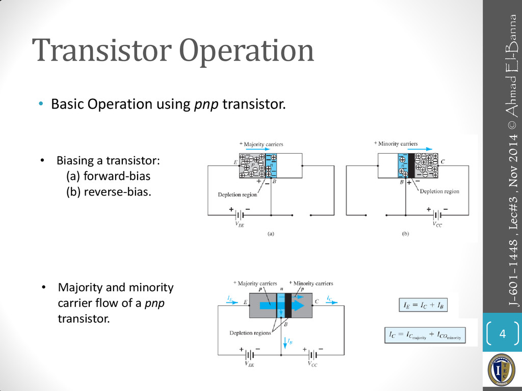
Transistor Operation • Basic Operation using pnp transistor. 4 •
Majority and minority carrier flow of a pnp transistor. • Biasing a transistor: (a) forward-bias (b) reverse-bias. J-601-1448 , Lec#3 , Nov 2014 © Ahmad El-Banna
BJT CONFIGURATIONS • Common Base • Common Emitter • Common
Collector 5 J-601-1448 , Lec#3 , Nov 2014 © Ahmad El-Banna
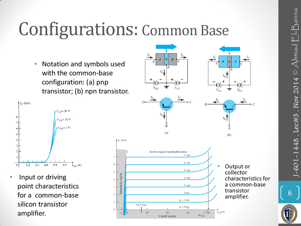
Configurations: Common Base • Notation and symbols used with the
common-base configuration: (a) pnp transistor; (b) npn transistor. 6 • Input or driving point characteristics for a common-base silicon transistor amplifier. • Output or collector characteristics for a common-base transistor amplifier. J-601-1448 , Lec#3 , Nov 2014 © Ahmad El-Banna
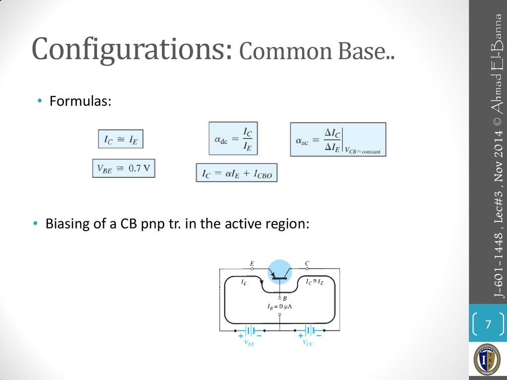
Configurations: Common Base.. • Formulas: 7 • Biasing of a
CB pnp tr. in the active region: J-601-1448 , Lec#3 , Nov 2014 © Ahmad El-Banna
Configurations: Common Emitter 8 • Notation and symbols used with
the common-emitter configuration: (a) pnp transistor (b) npn transistor. • Characteristics of a silicon transistor in the common- emitter configuration: (a) collector characteristics (b) base characteristics. J-601-1448 , Lec#3 , Nov 2014 © Ahmad El-Banna
Configurations: Common Emitter.. 9 • Formulas: • Biasing of a
CE npn tr. in the active region: J-601-1448 , Lec#3 , Nov 2014 © Ahmad El-Banna
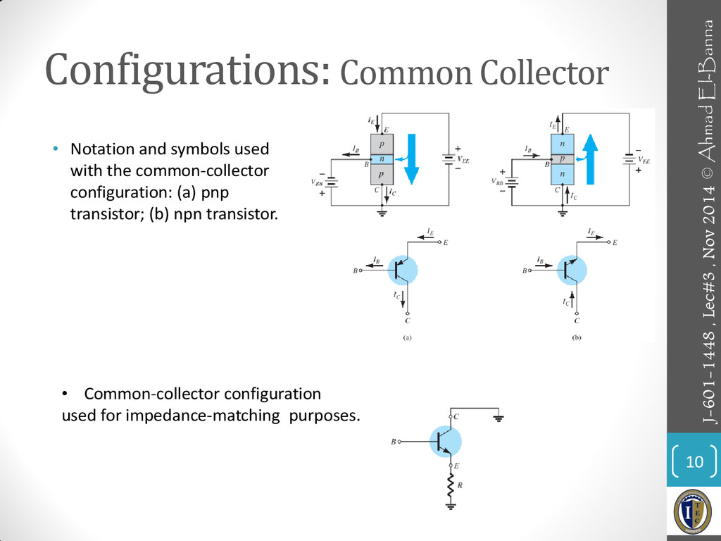
Configurations: Common Collector 10 • Notation and symbols used with
the common-collector configuration: (a) pnp transistor; (b) npn transistor. • Common-collector configuration used for impedance-matching purposes. J-601-1448 , Lec#3 , Nov 2014 © Ahmad El-Banna
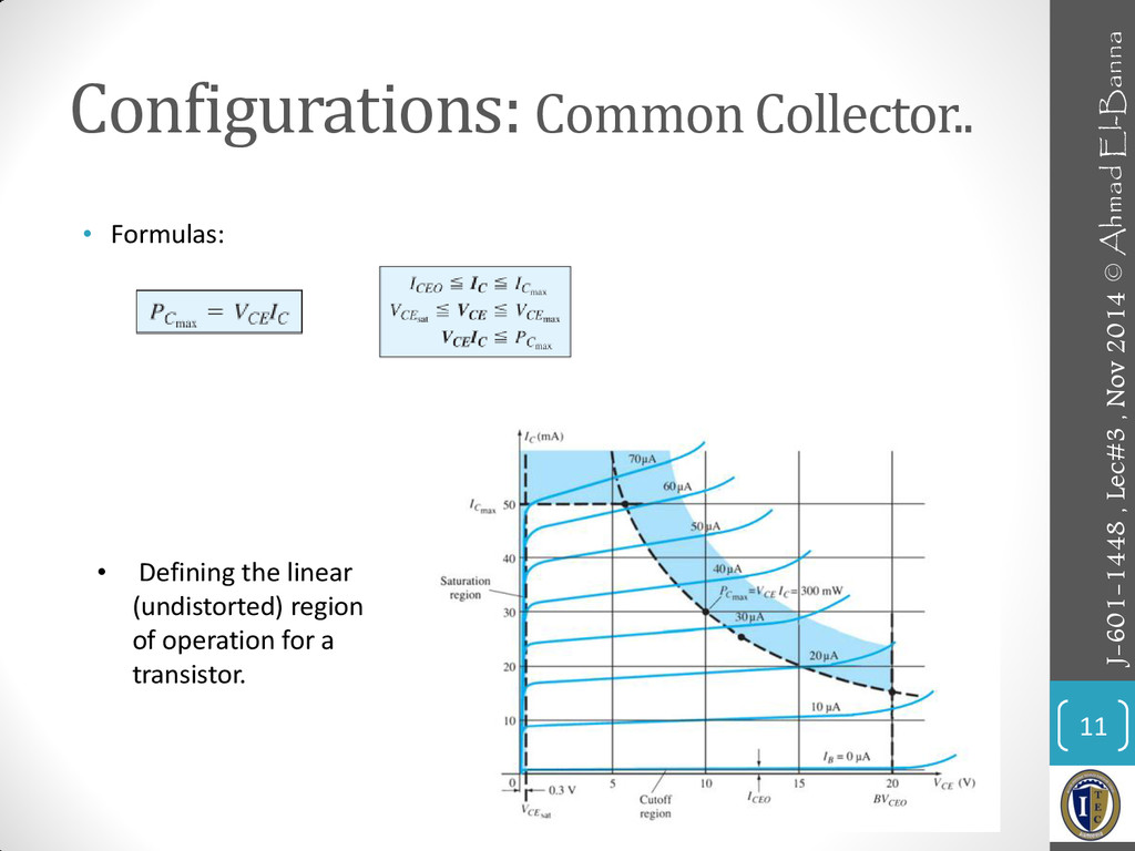
Configurations: Common Collector.. 11 • Defining the linear (undistorted) region
of operation for a transistor. • Formulas: J-601-1448 , Lec#3 , Nov 2014 © Ahmad El-Banna
PRACTICAL VIEW • Transistor Spec. Sheets • Transistor Testing •
Transistor Casing and terminals identification • Transistor Development 12 J-601-1448 , Lec#3 , Nov 2014 © Ahmad El-Banna
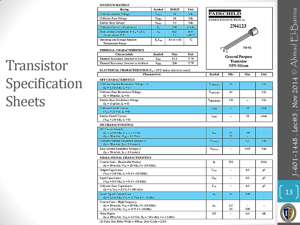
Transistor Specification Sheets 13 J-601-1448 , Lec#3 , Nov 2014
© Ahmad El-Banna
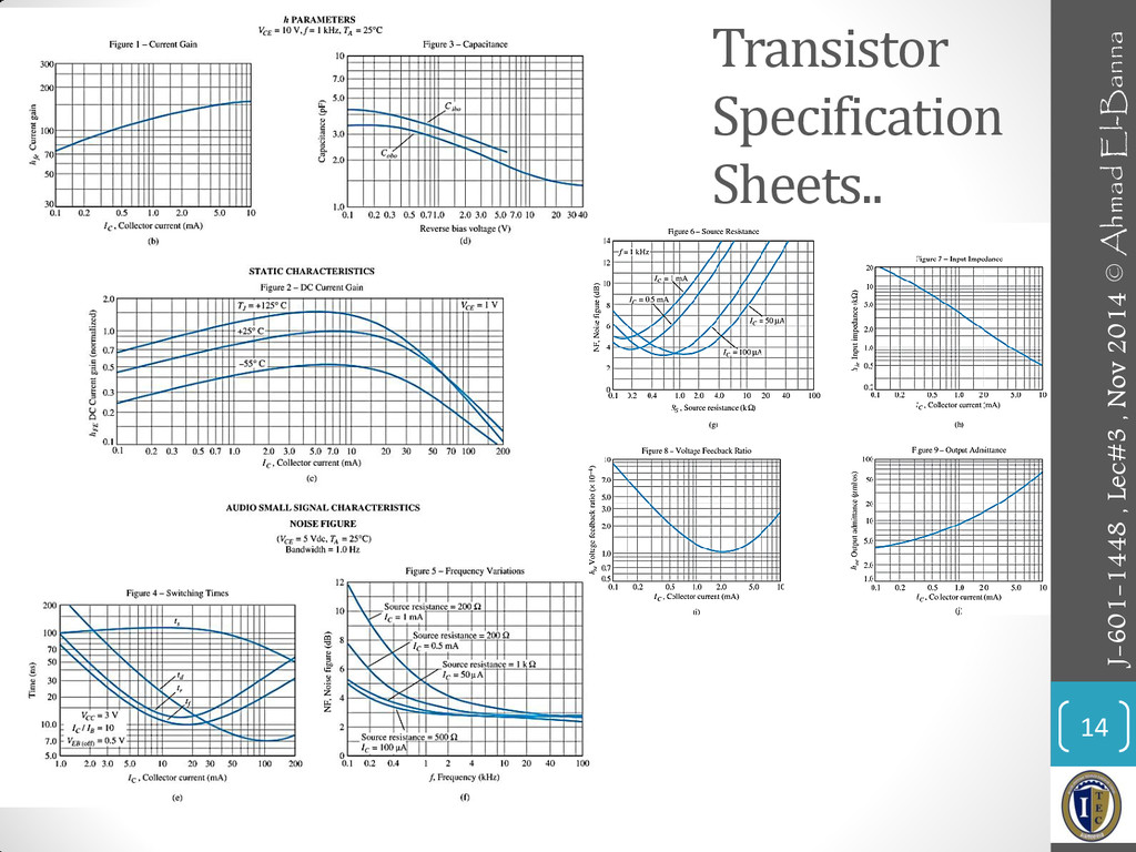
Transistor Specification Sheets.. 14 J-601-1448 , Lec#3 , Nov 2014
© Ahmad El-Banna
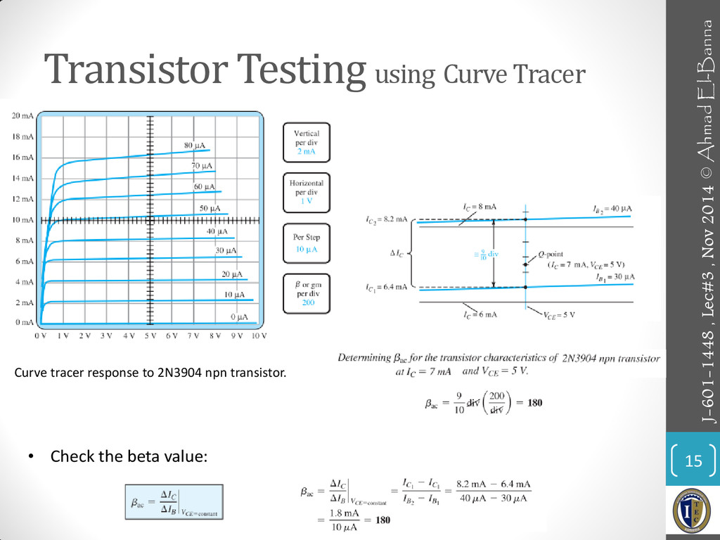
Transistor Testing using Curve Tracer 15 • Check the beta
value: Curve tracer response to 2N3904 npn transistor. J-601-1448 , Lec#3 , Nov 2014 © Ahmad El-Banna
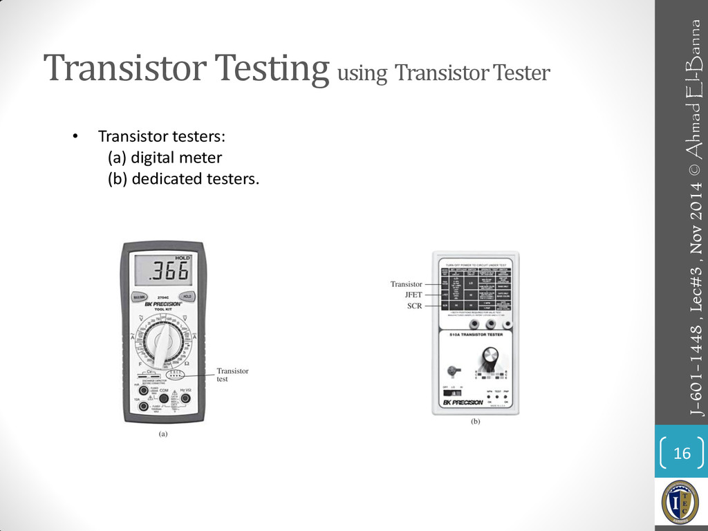
Transistor Testing using Transistor Tester 16 • Transistor testers: (a)
digital meter (b) dedicated testers. J-601-1448 , Lec#3 , Nov 2014 © Ahmad El-Banna
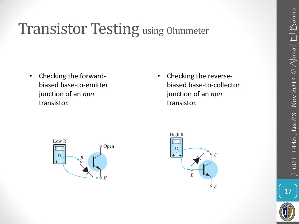
Transistor Testing using Ohmmeter 17 • Checking the forward- biased
base-to-emitter junction of an npn transistor. • Checking the reverse- biased base-to-collector junction of an npn transistor. J-601-1448 , Lec#3 , Nov 2014 © Ahmad El-Banna
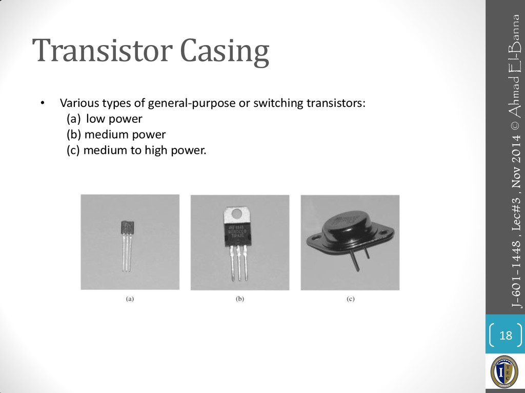
Transistor Casing 18 • Various types of general-purpose or switching
transistors: (a) low power (b) medium power (c) medium to high power. J-601-1448 , Lec#3 , Nov 2014 © Ahmad El-Banna
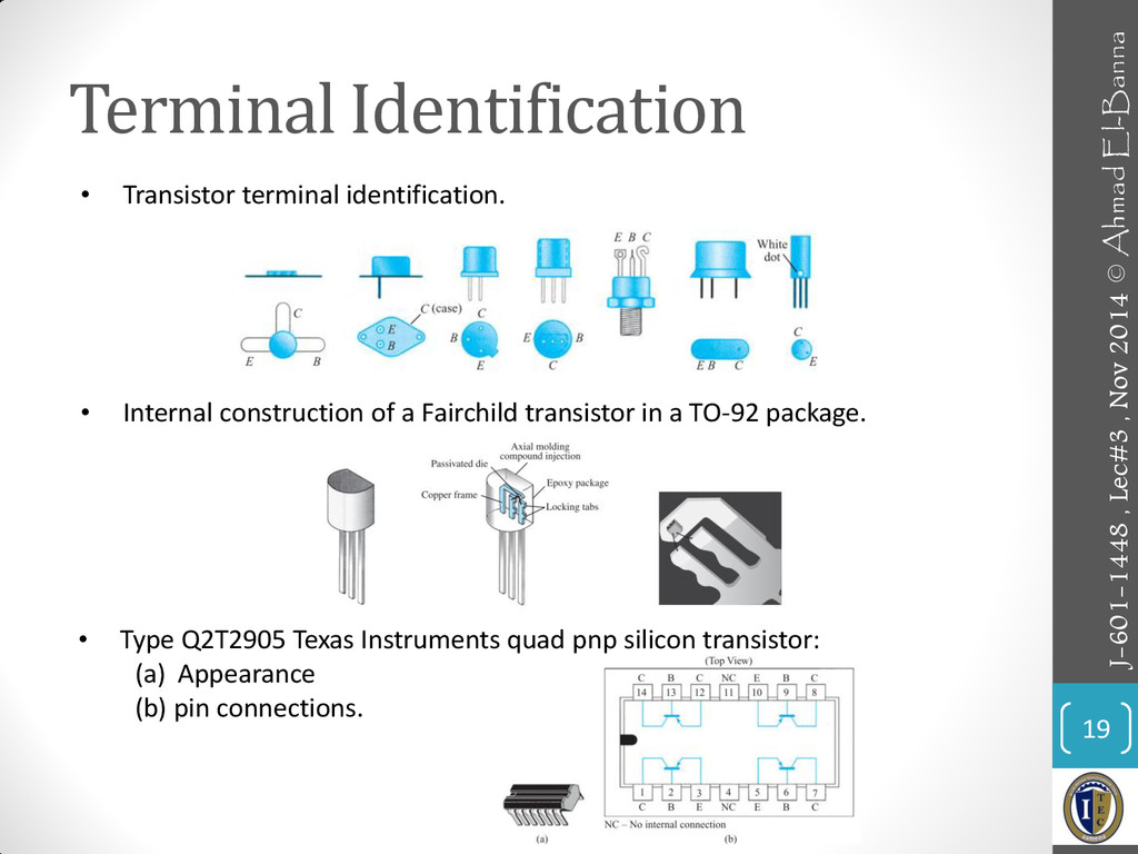
Terminal Identification 19 • Transistor terminal identification. • Internal construction
of a Fairchild transistor in a TO-92 package. • Type Q2T2905 Texas Instruments quad pnp silicon transistor: (a) Appearance (b) pin connections. J-601-1448 , Lec#3 , Nov 2014 © Ahmad El-Banna
TRANSISTOR DC BIAS CONFIGURATIONS • Fixed-Bias Configuration • Voltage-Divider Bias
Configuration • Emitter-Follower Configuration 20 • Biasing means applying of dc voltages to establish a fixed level of current and voltage. >>> Q-Point J-601-1448 , Lec#3 , Nov 2014 © Ahmad El-Banna
Fixed-Bias Configuration 21 • Fixed-bias circuit. • DC equivalent ct.
• Base–emitter loop. • Collector–emitter loop. J-601-1448 , Lec#3 , Nov 2014 © Ahmad El-Banna
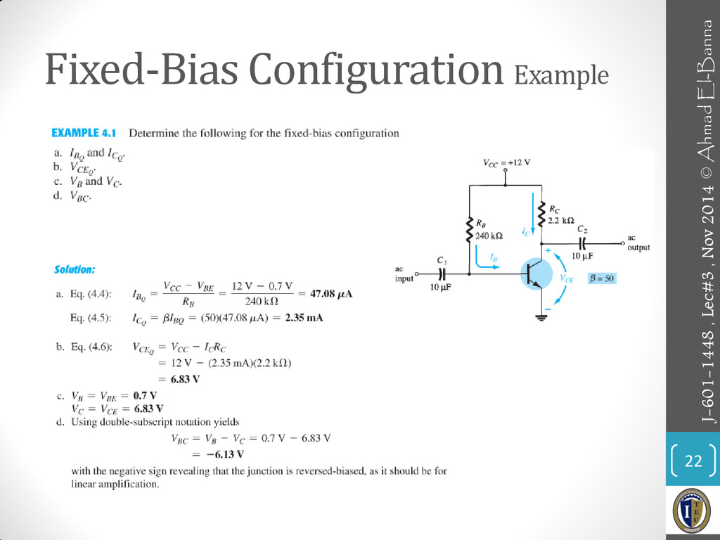
Fixed-Bias Configuration Example 22 J-601-1448 , Lec#3 , Nov 2014
© Ahmad El-Banna
Fixed-Bias Configuration ... 23 • Load Line Analysis J-601-1448 ,
Lec#3 , Nov 2014 © Ahmad El-Banna Saturation Current
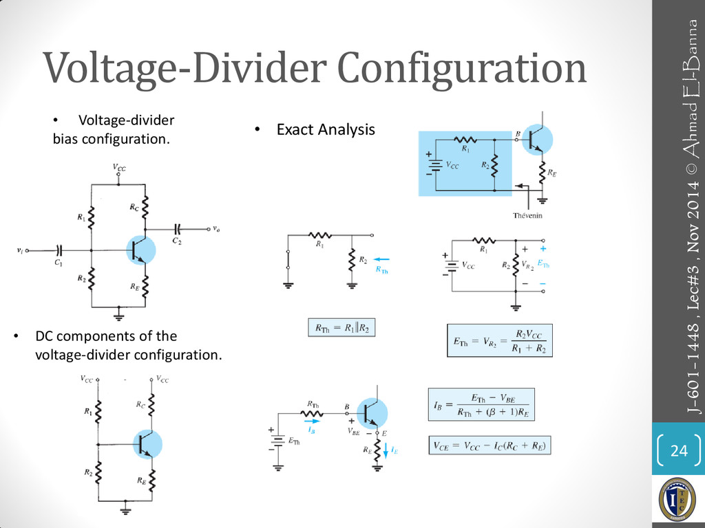
Voltage-Divider Configuration 24 • Exact Analysis • Voltage-divider bias configuration.
• DC components of the voltage-divider configuration. J-601-1448 , Lec#3 , Nov 2014 © Ahmad El-Banna
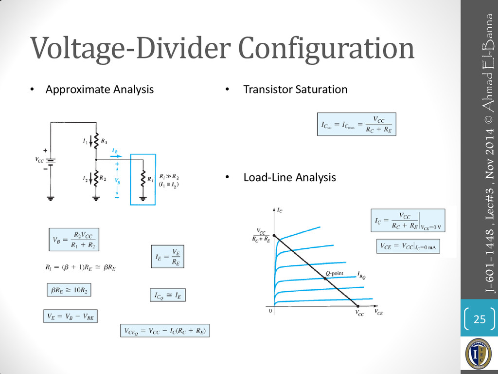
Voltage-Divider Configuration 25 • Approximate Analysis • Transistor Saturation •
Load-Line Analysis J-601-1448 , Lec#3 , Nov 2014 © Ahmad El-Banna
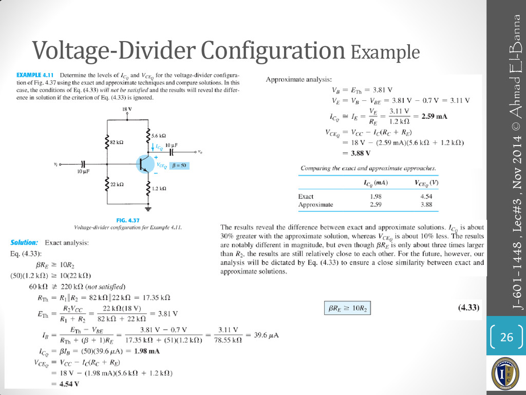
Voltage-Divider Configuration Example 26 J-601-1448 , Lec#3 , Nov 2014
© Ahmad El-Banna
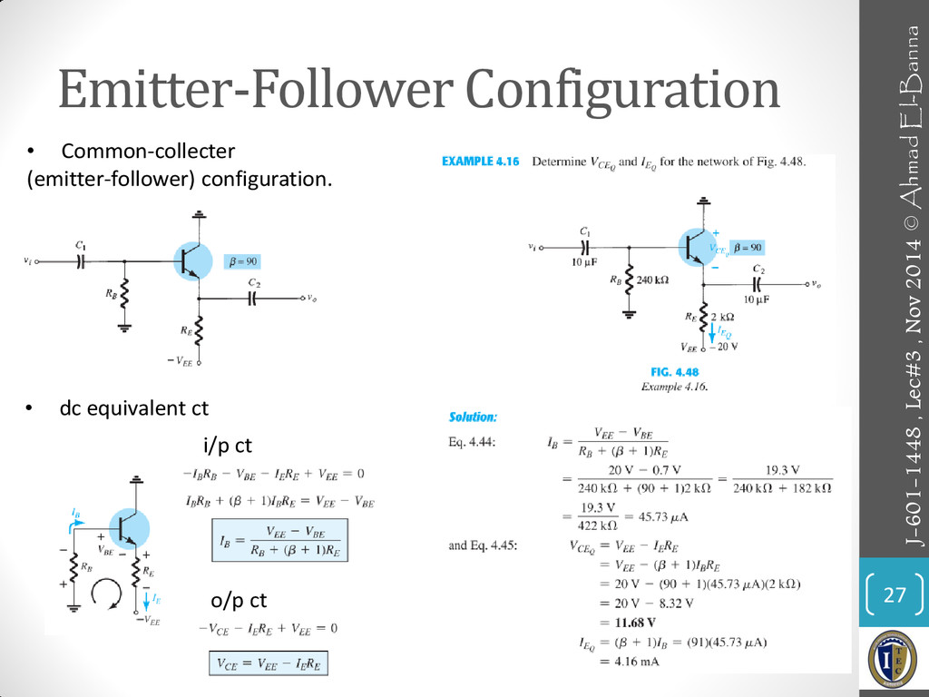
Emitter-Follower Configuration 27 i/p ct o/p ct • dc equivalent
ct • Common-collecter (emitter-follower) configuration. J-601-1448 , Lec#3 , Nov 2014 © Ahmad El-Banna
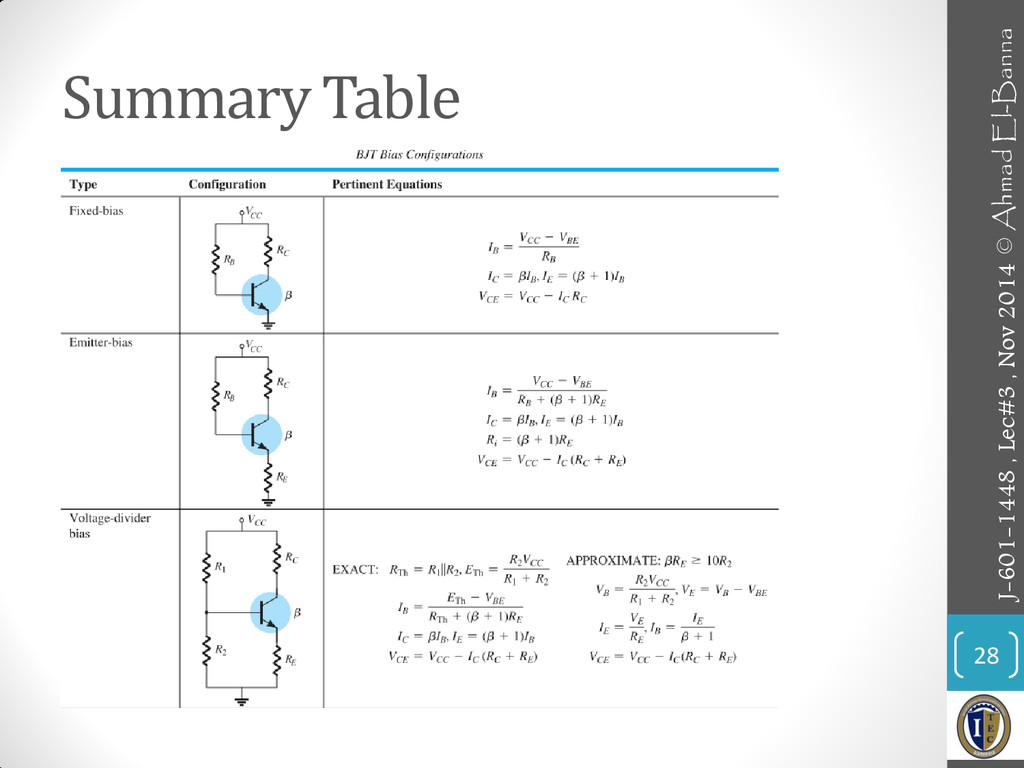
Summary Table 28 J-601-1448 , Lec#3 , Nov 2014 ©
Ahmad El-Banna
Summary Table.. 29 J-601-1448 , Lec#3 , Nov 2014 ©
Ahmad El-Banna
DESIGN OPERATION 30 J-601-1448 , Lec#3 , Nov 2014 ©
Ahmad El-Banna
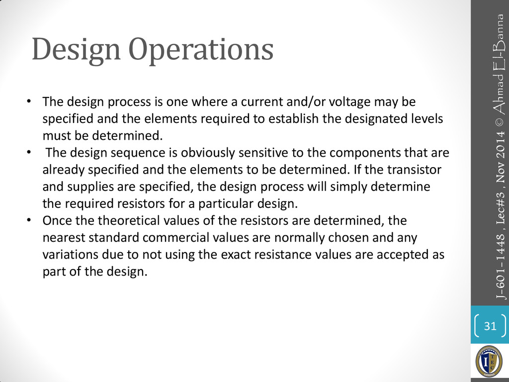
Design Operations 31 • The design process is one where
a current and/or voltage may be specified and the elements required to establish the designated levels must be determined. • The design sequence is obviously sensitive to the components that are already specified and the elements to be determined. If the transistor and supplies are specified, the design process will simply determine the required resistors for a particular design. • Once the theoretical values of the resistors are determined, the nearest standard commercial values are normally chosen and any variations due to not using the exact resistance values are accepted as part of the design. J-601-1448 , Lec#3 , Nov 2014 © Ahmad El-Banna
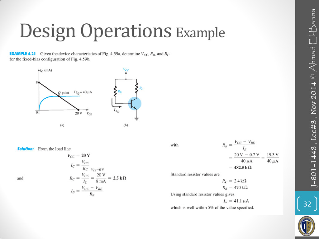
Design Operations Example 32 J-601-1448 , Lec#3 , Nov 2014
© Ahmad El-Banna
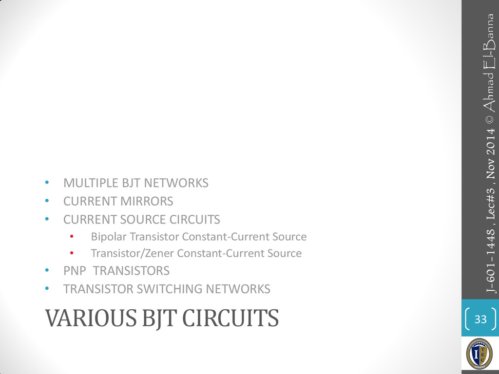
VARIOUS BJT CIRCUITS • MULTIPLE BJT NETWORKS • CURRENT MIRRORS
• CURRENT SOURCE CIRCUITS • Bipolar Transistor Constant-Current Source • Transistor/Zener Constant-Current Source • PNP TRANSISTORS • TRANSISTOR SWITCHING NETWORKS 33 J-601-1448 , Lec#3 , Nov 2014 © Ahmad El-Banna
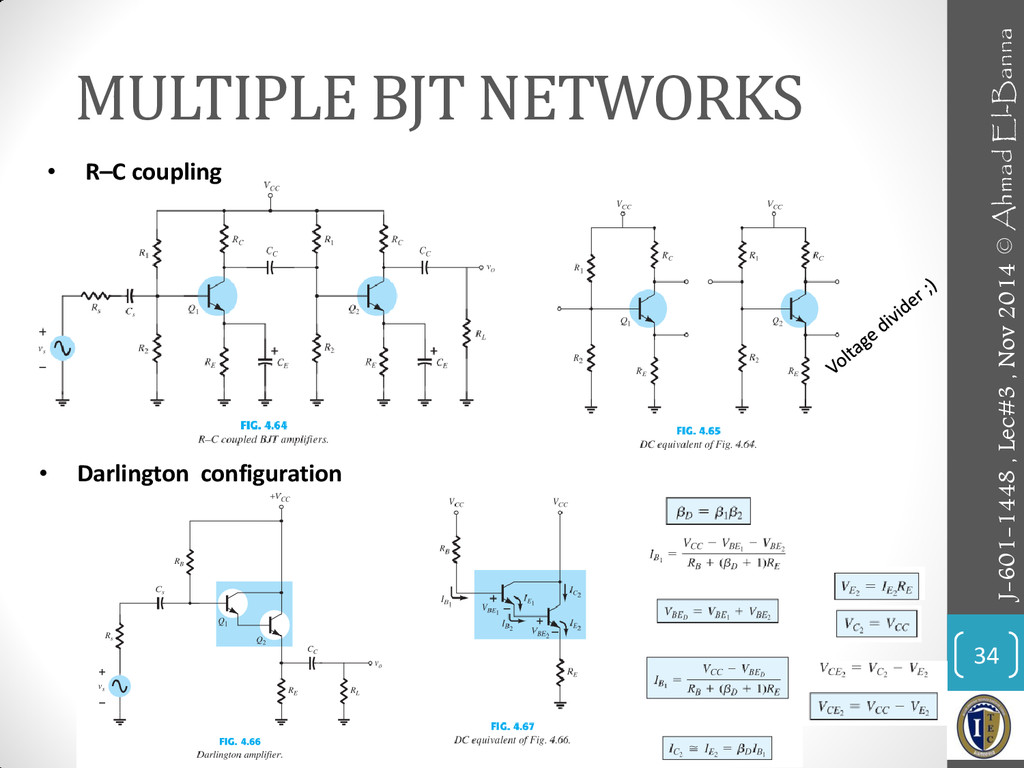
MULTIPLE BJT NETWORKS 34 • R–C coupling • Darlington configuration
J-601-1448 , Lec#3 , Nov 2014 © Ahmad El-Banna
CURRENT MIRRORS 35 J-601-1448 , Lec#3 , Nov 2014 ©
Ahmad El-Banna
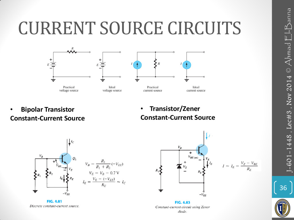
CURRENT SOURCE CIRCUITS 36 • Bipolar Transistor Constant-Current Source •
Transistor/Zener Constant-Current Source J-601-1448 , Lec#3 , Nov 2014 © Ahmad El-Banna
pnp TRANSISTORS 37 TRANSISTOR SWITCHING NETWORKS J-601-1448 , Lec#3 ,
Nov 2014 © Ahmad El-Banna
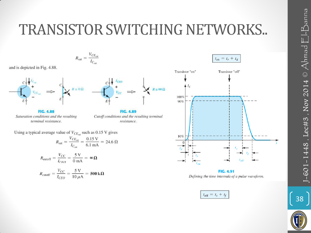
TRANSISTOR SWITCHING NETWORKS.. 38 J-601-1448 , Lec#3 , Nov 2014
© Ahmad El-Banna
TROUBLESHOOTING TECHNIQUES 39 J-601-1448 , Lec#3 , Nov 2014 ©
Ahmad El-Banna
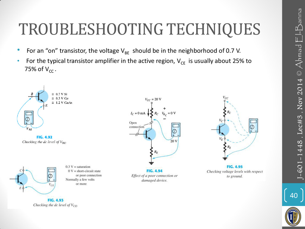
TROUBLESHOOTING TECHNIQUES • For an “on” transistor, the voltage VBE
should be in the neighborhood of 0.7 V. • For the typical transistor amplifier in the active region, VCE is usually about 25% to 75% of VCC . 40 J-601-1448 , Lec#3 , Nov 2014 © Ahmad El-Banna
PRACTICAL APPLICATION • BJT Diode Usage and Protective Capabilities •
Relay Driver • Alarm System with a CCS • Voltage Level Indicator • Logic Gates 41 J-601-1448 , Lec#3 , Nov 2014 © Ahmad El-Banna
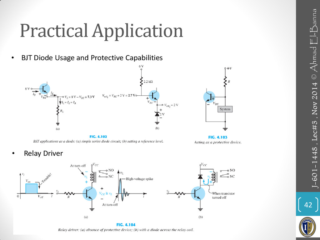
Practical Application 42 • BJT Diode Usage and Protective Capabilities
• Relay Driver J-601-1448 , Lec#3 , Nov 2014 © Ahmad El-Banna
Practical Application… 43 • Alarm System with a CCS •
Voltage Level Indicator J-601-1448 , Lec#3 , Nov 2014 © Ahmad El-Banna
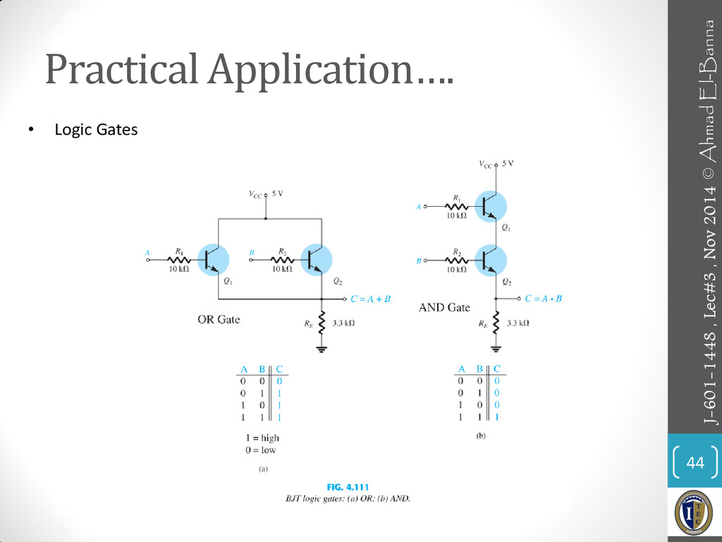
Practical Application…. 44 • Logic Gates J-601-1448 , Lec#3 ,
Nov 2014 © Ahmad El-Banna
• For more details, refer to: • Chapter 3 &
4, Electronic Devices and Circuits, Boylestad. • The lecture is available online at: • https://speakerdeck.com/ahmad_elbanna • For inquires, send to: •
[email protected]
45 J-601-1448 , Lec#3 , Nov 2014 © Ahmad El-Banna