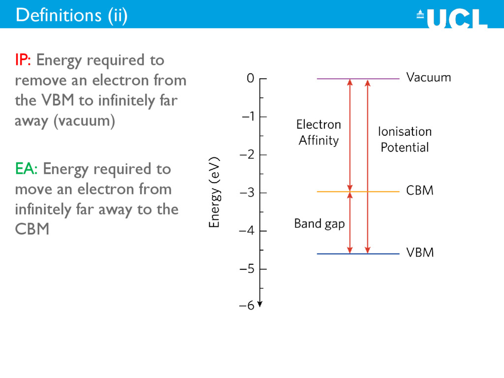
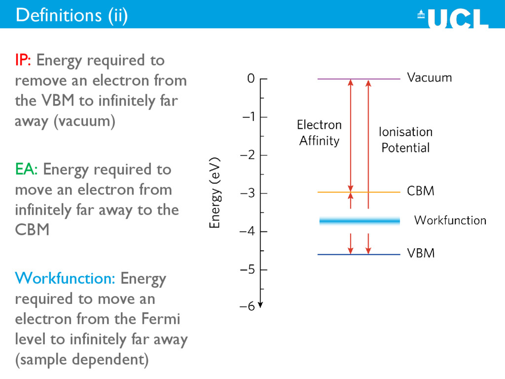
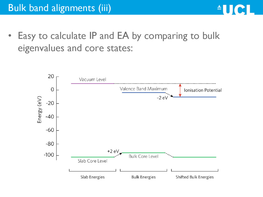
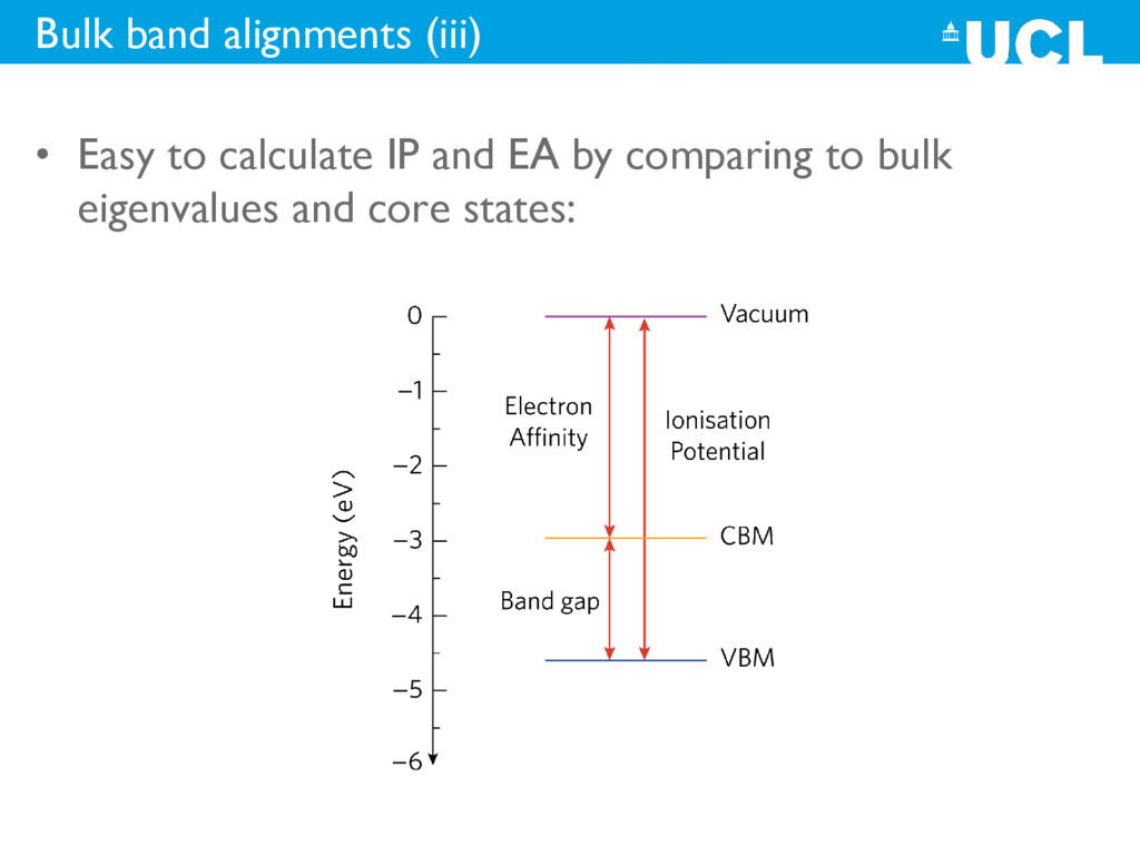
the VBM to infinitely far away (vacuum) EA: Energy required to move an electron from infinitely far away to the CBM Workfunction: Energy required to move an electron from the Fermi level to infinitely far away (sample dependent)
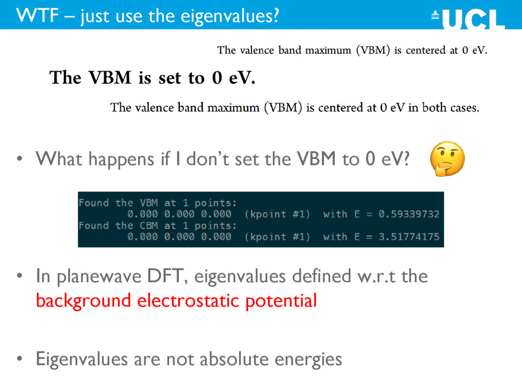
0 eV? • In planewave DFT, eigenvalues defined w.r.t the background electrostatic potential • Eigenvalues are not absolute energies WTF – just use the eigenvalues? 7
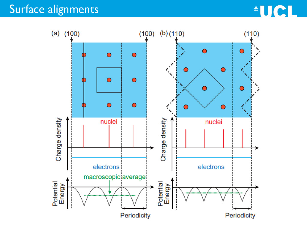
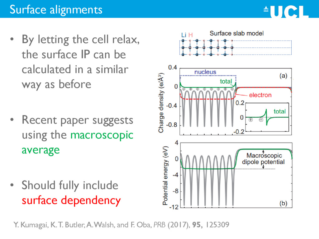
IP can be calculated in a similar way as before • Recent paper suggests using the macroscopic average • Should fully include surface dependency Y. Kumagai, K. T. Butler, A. Walsh, and F. Oba, PRB (2017), 95, 125309
• Bulk band alignment easy to calculate; surface alignment more expensive Note: Experimentally available via X-ray photoelectron spectroscopy (XPS) or Kelvin probe microscopy Warning: results are only as good as your DFT Functional
![E-mail: [email protected] @alexganose Theory of Ionization Potentials and Electron Affinities](https://files.speakerdeck.com/presentations/cd191522e3fb44b18011be16435f8cec/slide_0.jpg)